What is Cathodoluminescence? - DELMIC

In cathodoluminescence imaging, an electron beam is used to excite nanostructures and the cathodoluminescence detector is subsequently used to detect the produced light. Cathodoluminescence emission can be used to explore many fundamental properties of matter. It can be used to study light transport, scattering, electronic structure of a material, resonant phenomena and much more. It thus presents a valuable source of information for fundamental research as well as applied research with a direct link to industry. The SPARC is a high-performance cathodoluminescence detection system that is designed and produced by Delmic. With this system, Delmic offers a unique solution for cathodoluminescence imaging. In this presentation, we share the knowledge about the cathodoluminescence technique and point out the key advantages of using cathodoluminescence imaging in different areas. For questions about cathodoluminescence and the SPARC, please leave a comment below or visit www.delmic.com and send us a message.

Recomendados
Más contenido relacionado
La actualidad más candente
La actualidad más candente (20)
Similar a What is Cathodoluminescence? - DELMIC
Similar a What is Cathodoluminescence? - DELMIC (20)
Último
Último (20)
What is Cathodoluminescence? - DELMIC
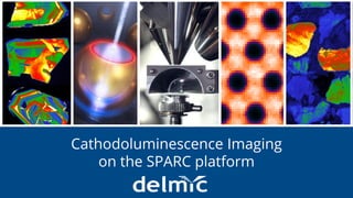
- 1. Integration without compromise Cathodoluminescence Imaging on the SPARC platform
- 2. Cathodoluminescence • Cathodoluminescence (CL) is the process whereby light is generated when an electron beam hits a specimen. • Cathodoluminescence imaging is an analytical technique that combines functional optical information with the superior spatial resolution of electron microscopy.
- 3. Why Cathodoluminescence is important? Cathodoluminescence emission is used to study the fundamental properties of matter: • Light transport • Scattering • Electronic structure of a material (e.g. bandgap, defects) • Resonant phenomena Cathodoluminescence is therefore a valuable source of information for fundamental research, as well as applied research in industry (e.g. metrology, failure analysis)
- 4. Key advantages of Cathodoluminescence imaging Using electrons as an optical excitation source has several advantages: • Overcoming the diffraction limit: high excitation resolution (1 – 10 nm precision) • Measurements are performed with an electron microscope environment • Can be used to correlate nanoscale geometrical features with the optical response
- 5. Application Areas - Geology CL presents a valuable technique for fundamental sedimentary, metamorphic, and igneous rock studies but also for more applied studies on ores, precious gems, reservoir rocks, and construction materials.
- 6. Application Areas - Nanophotonics CL imaging is a powerful method for studying optical phenomena at the nanoscale. It is applicable to metallic as well as dielectric and semiconductor nanostructures. These structures find applications in (bio)sensing, fluorescence enhancement, non-linear optics, low-threshold steam generation, LED’s, solar cells, integrated photonics, lasers and much more.
- 7. Application Areas – Materials Science CL can be used to study ceramics, dielectrics and semiconductors (both in bulk and nanostructur ed materials) and to determine their light-emitting properties at the nanoscale. This is useful for many functional materials, including scintillators, phosphors, high-power electr onics light-emitting-diodes, diode lasers and solar cells.
- 8. Cathodoluminescence SEM – The SPARC The SPARC is a high-performance Cathodoluminescence Scanning Electron Microscope (SEM) that is produced and designed by Delmic. The system is ideal for the optimal collection and detection of cathodoluminescence emission, enabling fast and sensitive material characterization at the nanoscale. SPARC SPARC Compact
- 9. Highlights of the SPARC • Modular design • UV/VIS/NIR optics and detectors • Calibration light source • Fiber coupling • Photomultiplier tube for intensity mapping Spectrograph Optics Optical module Grating turret
- 10. Integration without compromise DELMIC B.V. Address: Kanaalweg 4, 2628 EB, Delft, The Netherlands Website: www.delmic.com Telephone: +31 (0)15 744 01 58 Email: info@delmic.com Please visit Delmic’s website to learn more about the unique solution for cathodoluminescene imaging.