SlideShare una empresa de Scribd logo
1 de 8
BASIC ELECTRONIC CIRCUITS/19EC203/ E.Divya/ Unit 2/ CE,CB & CC CONFIGURATIONS
CE, CB, CC configurations and characteristics
Introduction
 We know that generally the transistor has three terminals –
emitter (E), base (B) and collector. But in the circuit
connections we need four terminals, two terminals for
input and another two terminals for output.
 To overcome these problems we use one terminal as
common for both input and output actions.
 Using this property we construct the circuits and these
structures are called transistor configurations.
BASIC ELECTRONIC CIRCUITS/19EC203/ E.Divya/ Unit 2/ CE,CB & CC CONFIGURATIONS
Generally there are three different configurations of transistors and
they are common base (CB) configuration, common collector (CC)
configuration and common emitter (CE) configuration.
The behaviour of these three different configurations of transistors
with respect to gain is given below.
1. Common Base (CB) Configuration: no current gain but
voltage gain
2. Common Collector (CC) Configuration: current gain but no
voltage gain
3. Common Emitter (CE) Configuration: current gain and
voltage gain
BASIC ELECTRONIC CIRCUITS/19EC203/ E.Divya/ Unit 2/ CE,CB & CC CONFIGURATIONS
Common Base (CB) Configuration:
In CB Configuration, the base terminal of the transistor will be
connected common between the output and the input terminals.
BASIC ELECTRONIC CIRCUITS/19EC203/ E.Divya/ Unit 2/ CE,CB & CC CONFIGURATIONS
 The configuration name itself indicates the common
terminal.
 Here the input is applied between the base and emitter
terminals and the corresponding output signal is taken
between the base and collector terminals with the base
terminal grounded.
 Here the input parameters are VEB and IE and the output
parameters are VCB and IC.
 The input current flowing into the emitter terminal must be
higher than the base current and collector current to operate
the transistor, therefore the output collector current is less
than the input emitter current.
BASIC ELECTRONIC CIRCUITS/19EC203/ E.Divya/ Unit 2/ CE,CB & CC CONFIGURATIONS
 The current gain is generally equal or less than to unity for
this type of configuration.
 This type of configuration has high resistance gain i.e. ratio of
output resistance to input resistance is high.
 The voltage gain for this configuration of circuit is given
below.
AV = Vout/Vin = (IC*RL) / (IE*Rin)
 Current gain in common base configuration is given as
α = Output current/Input current
α = IC/IE
BASIC ELECTRONIC CIRCUITS/19EC203/ E.Divya/ Unit 2/ CE,CB & CC CONFIGURATIONS
Input Characteristics
 Input characteristics are obtained between input current and
input voltage with constant output voltage.
 First keep the output voltage VCB constant and vary the input
voltage VEB for different points then at each point record the
input current IE value.
 Repeat the same process at different output voltage levels.
BASIC ELECTRONIC CIRCUITS/19EC203/ E.Divya/ Unit 2/ CE,CB & CC CONFIGURATIONS
Output Characteristics
 It is defined as the characteristic curve drawn between output
voltage to output current whereas input current is constant.
 To determine output characteristics, the emitter current IE is kept
constant at zero and collector current Ic is increased from zero by
increasing VCB.This is repeated for higher fixed values of IE.
BASIC ELECTRONIC CIRCUITS/19EC203/ E.Divya/ Unit 2/ CE,CB & CC CONFIGURATIONS
 In CB configuration a variation of the base-collector voltage
results in a variation of the quasi- neutral width in the base.
 The gradient of the minority-carrier density in the base
therefore changes, yielding an increased collector current as
the collector-base current is increased. This effect is referred
to as the Early effect.

Más contenido relacionado

La actualidad más candente

Zener Diode Full Presentation
Zener Diode Full Presentation Zener Diode Full Presentation
Zener Diode Full Presentation Adeel Rasheed
 
Bio-polar junction transistor (edc)
Bio-polar junction transistor  (edc)Bio-polar junction transistor  (edc)
Bio-polar junction transistor (edc)Abhinay Potlabathini
 
Transistor Configuration
Transistor Configuration Transistor Configuration
Transistor Configuration Smit Shah
 
TRANSISTORS
 TRANSISTORS TRANSISTORS
TRANSISTORSAJAL A J
 
Rectifier and Filter circuits (chapter14)
Rectifier and Filter circuits (chapter14)Rectifier and Filter circuits (chapter14)
Rectifier and Filter circuits (chapter14)DHARUN MUGHILAN
 
Op amp(operational amplifier)
Op amp(operational amplifier)Op amp(operational amplifier)
Op amp(operational amplifier)Kausik das
 
Dc Motor Construction and Working
Dc Motor Construction and WorkingDc Motor Construction and Working
Dc Motor Construction and WorkingSourabh sharma
 
Operational amplifier
Operational amplifierOperational amplifier
Operational amplifierUnsa Shakir
 
Field Effect Transistor ppt
Field Effect Transistor pptField Effect Transistor ppt
Field Effect Transistor pptSameeksha Verma
 
Class a power amplifiers
Class a power amplifiersClass a power amplifiers
Class a power amplifiersAdarsh Raj
 
Bipolar junction transistors working principle and applications
Bipolar junction transistors working principle and applicationsBipolar junction transistors working principle and applications
Bipolar junction transistors working principle and applicationselprocus
 

La actualidad más candente (20)

Zener Diode Full Presentation
Zener Diode Full Presentation Zener Diode Full Presentation
Zener Diode Full Presentation
 
Clampers
ClampersClampers
Clampers
 
Bio-polar junction transistor (edc)
Bio-polar junction transistor  (edc)Bio-polar junction transistor  (edc)
Bio-polar junction transistor (edc)
 
Transistor biasing
Transistor biasing Transistor biasing
Transistor biasing
 
Transistor Configuration
Transistor Configuration Transistor Configuration
Transistor Configuration
 
Transistor configurations
Transistor configurationsTransistor configurations
Transistor configurations
 
TRANSISTORS
 TRANSISTORS TRANSISTORS
TRANSISTORS
 
Rectifier and Filter circuits (chapter14)
Rectifier and Filter circuits (chapter14)Rectifier and Filter circuits (chapter14)
Rectifier and Filter circuits (chapter14)
 
Transistor basics
Transistor   basicsTransistor   basics
Transistor basics
 
Op amp(operational amplifier)
Op amp(operational amplifier)Op amp(operational amplifier)
Op amp(operational amplifier)
 
JFET
JFETJFET
JFET
 
Dc Motor Construction and Working
Dc Motor Construction and WorkingDc Motor Construction and Working
Dc Motor Construction and Working
 
Operational amplifier
Operational amplifierOperational amplifier
Operational amplifier
 
Field Effect Transistor
Field Effect TransistorField Effect Transistor
Field Effect Transistor
 
Op amp
Op ampOp amp
Op amp
 
Clipper and clampers
Clipper and clampersClipper and clampers
Clipper and clampers
 
Field Effect Transistor ppt
Field Effect Transistor pptField Effect Transistor ppt
Field Effect Transistor ppt
 
Class a power amplifiers
Class a power amplifiersClass a power amplifiers
Class a power amplifiers
 
Dc motor ppt
Dc motor pptDc motor ppt
Dc motor ppt
 
Bipolar junction transistors working principle and applications
Bipolar junction transistors working principle and applicationsBipolar junction transistors working principle and applications
Bipolar junction transistors working principle and applications
 

Similar a CB CONFIGURATION.pptx

Electronics 1 : Chapter # 06 : Bipolar Junction Transistor
Electronics 1 : Chapter # 06 : Bipolar Junction TransistorElectronics 1 : Chapter # 06 : Bipolar Junction Transistor
Electronics 1 : Chapter # 06 : Bipolar Junction TransistorSk_Group
 
BJT by Emroz Sardar.pptx
BJT by Emroz Sardar.pptxBJT by Emroz Sardar.pptx
BJT by Emroz Sardar.pptxEmroz Sardar
 
Common Emitter Configuration and Collector Curve
Common Emitter Configuration and Collector CurveCommon Emitter Configuration and Collector Curve
Common Emitter Configuration and Collector CurveZeeshan Rafiq
 
addeunit-2-191121144848.pptx
addeunit-2-191121144848.pptxaddeunit-2-191121144848.pptx
addeunit-2-191121144848.pptxKUMARS641064
 
Bipolar Transistor and its configurations
Bipolar Transistor and its configurationsBipolar Transistor and its configurations
Bipolar Transistor and its configurationsSyedAliAsdaque
 
Phy 4240 lec (9) and (10)
Phy 4240 lec (9) and (10)Phy 4240 lec (9) and (10)
Phy 4240 lec (9) and (10)Dr. Abeer Kamal
 
BJT BIASING-SOWMIYA.pdf
BJT BIASING-SOWMIYA.pdfBJT BIASING-SOWMIYA.pdf
BJT BIASING-SOWMIYA.pdfGunaG14
 
Transistors & Oscillators by Er. Swapnil Kaware
Transistors & Oscillators by Er. Swapnil KawareTransistors & Oscillators by Er. Swapnil Kaware
Transistors & Oscillators by Er. Swapnil KawareProf. Swapnil V. Kaware
 
Transistor, MOSFET and Operational Amplr
Transistor, MOSFET and Operational AmplrTransistor, MOSFET and Operational Amplr
Transistor, MOSFET and Operational AmplrHarshalVaidya11
 
Chapter 6: Bipolar Junction Transistors (BJTs)
Chapter 6: Bipolar Junction Transistors (BJTs)Chapter 6: Bipolar Junction Transistors (BJTs)
Chapter 6: Bipolar Junction Transistors (BJTs)JeremyLauKarHei
 

Similar a CB CONFIGURATION.pptx (20)

Bjt session 2
Bjt session 2Bjt session 2
Bjt session 2
 
RAGHU92.pptx
RAGHU92.pptxRAGHU92.pptx
RAGHU92.pptx
 
Electronics 1 : Chapter # 06 : Bipolar Junction Transistor
Electronics 1 : Chapter # 06 : Bipolar Junction TransistorElectronics 1 : Chapter # 06 : Bipolar Junction Transistor
Electronics 1 : Chapter # 06 : Bipolar Junction Transistor
 
BJT by Emroz Sardar.pptx
BJT by Emroz Sardar.pptxBJT by Emroz Sardar.pptx
BJT by Emroz Sardar.pptx
 
ADE unit 2 jntu hyderabad
ADE unit 2 jntu hyderabad ADE unit 2 jntu hyderabad
ADE unit 2 jntu hyderabad
 
Common Emitter Configuration and Collector Curve
Common Emitter Configuration and Collector CurveCommon Emitter Configuration and Collector Curve
Common Emitter Configuration and Collector Curve
 
Cbcs e1 unit 3
Cbcs e1 unit 3Cbcs e1 unit 3
Cbcs e1 unit 3
 
addeunit-2-191121144848.pptx
addeunit-2-191121144848.pptxaddeunit-2-191121144848.pptx
addeunit-2-191121144848.pptx
 
ppt_ae.pdf
ppt_ae.pdfppt_ae.pdf
ppt_ae.pdf
 
BJT & ITS BIASING
BJT & ITS BIASINGBJT & ITS BIASING
BJT & ITS BIASING
 
Bipolar Transistor and its configurations
Bipolar Transistor and its configurationsBipolar Transistor and its configurations
Bipolar Transistor and its configurations
 
Unit 2.pptx
Unit  2.pptxUnit  2.pptx
Unit 2.pptx
 
BJT.ppt
BJT.pptBJT.ppt
BJT.ppt
 
Phy 4240 lec (9) and (10)
Phy 4240 lec (9) and (10)Phy 4240 lec (9) and (10)
Phy 4240 lec (9) and (10)
 
Unit II.ppt
Unit II.pptUnit II.ppt
Unit II.ppt
 
BJT BIASING-SOWMIYA.pdf
BJT BIASING-SOWMIYA.pdfBJT BIASING-SOWMIYA.pdf
BJT BIASING-SOWMIYA.pdf
 
Ce configuration
Ce configurationCe configuration
Ce configuration
 
Transistors & Oscillators by Er. Swapnil Kaware
Transistors & Oscillators by Er. Swapnil KawareTransistors & Oscillators by Er. Swapnil Kaware
Transistors & Oscillators by Er. Swapnil Kaware
 
Transistor, MOSFET and Operational Amplr
Transistor, MOSFET and Operational AmplrTransistor, MOSFET and Operational Amplr
Transistor, MOSFET and Operational Amplr
 
Chapter 6: Bipolar Junction Transistors (BJTs)
Chapter 6: Bipolar Junction Transistors (BJTs)Chapter 6: Bipolar Junction Transistors (BJTs)
Chapter 6: Bipolar Junction Transistors (BJTs)
 

Último

PVC VS. FIBERGLASS (FRP) GRAVITY SEWER - UNI BELL
PVC VS. FIBERGLASS (FRP) GRAVITY SEWER - UNI BELLPVC VS. FIBERGLASS (FRP) GRAVITY SEWER - UNI BELL
PVC VS. FIBERGLASS (FRP) GRAVITY SEWER - UNI BELLManishPatel169454
 
Intze Overhead Water Tank Design by Working Stress - IS Method.pdf
Intze Overhead Water Tank  Design by Working Stress - IS Method.pdfIntze Overhead Water Tank  Design by Working Stress - IS Method.pdf
Intze Overhead Water Tank Design by Working Stress - IS Method.pdfSuman Jyoti
 
data_management_and _data_science_cheat_sheet.pdf
data_management_and _data_science_cheat_sheet.pdfdata_management_and _data_science_cheat_sheet.pdf
data_management_and _data_science_cheat_sheet.pdfJiananWang21
 
The Most Attractive Pune Call Girls Manchar 8250192130 Will You Miss This Cha...
The Most Attractive Pune Call Girls Manchar 8250192130 Will You Miss This Cha...The Most Attractive Pune Call Girls Manchar 8250192130 Will You Miss This Cha...
The Most Attractive Pune Call Girls Manchar 8250192130 Will You Miss This Cha...ranjana rawat
 
chapter 5.pptx: drainage and irrigation engineering
chapter 5.pptx: drainage and irrigation engineeringchapter 5.pptx: drainage and irrigation engineering
chapter 5.pptx: drainage and irrigation engineeringmulugeta48
 
Online banking management system project.pdf
Online banking management system project.pdfOnline banking management system project.pdf
Online banking management system project.pdfKamal Acharya
 
UNIT-V FMM.HYDRAULIC TURBINE - Construction and working
UNIT-V FMM.HYDRAULIC TURBINE - Construction and workingUNIT-V FMM.HYDRAULIC TURBINE - Construction and working
UNIT-V FMM.HYDRAULIC TURBINE - Construction and workingrknatarajan
 
Call Girls Pimpri Chinchwad Call Me 7737669865 Budget Friendly No Advance Boo...
Call Girls Pimpri Chinchwad Call Me 7737669865 Budget Friendly No Advance Boo...Call Girls Pimpri Chinchwad Call Me 7737669865 Budget Friendly No Advance Boo...
Call Girls Pimpri Chinchwad Call Me 7737669865 Budget Friendly No Advance Boo...roncy bisnoi
 
University management System project report..pdf
University management System project report..pdfUniversity management System project report..pdf
University management System project report..pdfKamal Acharya
 
Generative AI or GenAI technology based PPT
Generative AI or GenAI technology based PPTGenerative AI or GenAI technology based PPT
Generative AI or GenAI technology based PPTbhaskargani46
 
Thermal Engineering Unit - I & II . ppt
Thermal Engineering  Unit - I & II . pptThermal Engineering  Unit - I & II . ppt
Thermal Engineering Unit - I & II . pptDineshKumar4165
 
Call for Papers - Educational Administration: Theory and Practice, E-ISSN: 21...
Call for Papers - Educational Administration: Theory and Practice, E-ISSN: 21...Call for Papers - Educational Administration: Theory and Practice, E-ISSN: 21...
Call for Papers - Educational Administration: Theory and Practice, E-ISSN: 21...Christo Ananth
 
Call for Papers - International Journal of Intelligent Systems and Applicatio...
Call for Papers - International Journal of Intelligent Systems and Applicatio...Call for Papers - International Journal of Intelligent Systems and Applicatio...
Call for Papers - International Journal of Intelligent Systems and Applicatio...Christo Ananth
 
result management system report for college project
result management system report for college projectresult management system report for college project
result management system report for college projectTonystark477637
 
Double rodded leveling 1 pdf activity 01
Double rodded leveling 1 pdf activity 01Double rodded leveling 1 pdf activity 01
Double rodded leveling 1 pdf activity 01KreezheaRecto
 
Vivazz, Mieres Social Housing Design Spain
Vivazz, Mieres Social Housing Design SpainVivazz, Mieres Social Housing Design Spain
Vivazz, Mieres Social Housing Design Spaintimesproduction05
 

Último (20)

PVC VS. FIBERGLASS (FRP) GRAVITY SEWER - UNI BELL
PVC VS. FIBERGLASS (FRP) GRAVITY SEWER - UNI BELLPVC VS. FIBERGLASS (FRP) GRAVITY SEWER - UNI BELL
PVC VS. FIBERGLASS (FRP) GRAVITY SEWER - UNI BELL
 
Intze Overhead Water Tank Design by Working Stress - IS Method.pdf
Intze Overhead Water Tank  Design by Working Stress - IS Method.pdfIntze Overhead Water Tank  Design by Working Stress - IS Method.pdf
Intze Overhead Water Tank Design by Working Stress - IS Method.pdf
 
data_management_and _data_science_cheat_sheet.pdf
data_management_and _data_science_cheat_sheet.pdfdata_management_and _data_science_cheat_sheet.pdf
data_management_and _data_science_cheat_sheet.pdf
 
The Most Attractive Pune Call Girls Manchar 8250192130 Will You Miss This Cha...
The Most Attractive Pune Call Girls Manchar 8250192130 Will You Miss This Cha...The Most Attractive Pune Call Girls Manchar 8250192130 Will You Miss This Cha...
The Most Attractive Pune Call Girls Manchar 8250192130 Will You Miss This Cha...
 
chapter 5.pptx: drainage and irrigation engineering
chapter 5.pptx: drainage and irrigation engineeringchapter 5.pptx: drainage and irrigation engineering
chapter 5.pptx: drainage and irrigation engineering
 
Online banking management system project.pdf
Online banking management system project.pdfOnline banking management system project.pdf
Online banking management system project.pdf
 
UNIT-V FMM.HYDRAULIC TURBINE - Construction and working
UNIT-V FMM.HYDRAULIC TURBINE - Construction and workingUNIT-V FMM.HYDRAULIC TURBINE - Construction and working
UNIT-V FMM.HYDRAULIC TURBINE - Construction and working
 
(INDIRA) Call Girl Bhosari Call Now 8617697112 Bhosari Escorts 24x7
(INDIRA) Call Girl Bhosari Call Now 8617697112 Bhosari Escorts 24x7(INDIRA) Call Girl Bhosari Call Now 8617697112 Bhosari Escorts 24x7
(INDIRA) Call Girl Bhosari Call Now 8617697112 Bhosari Escorts 24x7
 
Call Girls Pimpri Chinchwad Call Me 7737669865 Budget Friendly No Advance Boo...
Call Girls Pimpri Chinchwad Call Me 7737669865 Budget Friendly No Advance Boo...Call Girls Pimpri Chinchwad Call Me 7737669865 Budget Friendly No Advance Boo...
Call Girls Pimpri Chinchwad Call Me 7737669865 Budget Friendly No Advance Boo...
 
University management System project report..pdf
University management System project report..pdfUniversity management System project report..pdf
University management System project report..pdf
 
Generative AI or GenAI technology based PPT
Generative AI or GenAI technology based PPTGenerative AI or GenAI technology based PPT
Generative AI or GenAI technology based PPT
 
Water Industry Process Automation & Control Monthly - April 2024
Water Industry Process Automation & Control Monthly - April 2024Water Industry Process Automation & Control Monthly - April 2024
Water Industry Process Automation & Control Monthly - April 2024
 
Thermal Engineering Unit - I & II . ppt
Thermal Engineering  Unit - I & II . pptThermal Engineering  Unit - I & II . ppt
Thermal Engineering Unit - I & II . ppt
 
Call for Papers - Educational Administration: Theory and Practice, E-ISSN: 21...
Call for Papers - Educational Administration: Theory and Practice, E-ISSN: 21...Call for Papers - Educational Administration: Theory and Practice, E-ISSN: 21...
Call for Papers - Educational Administration: Theory and Practice, E-ISSN: 21...
 
Call for Papers - International Journal of Intelligent Systems and Applicatio...
Call for Papers - International Journal of Intelligent Systems and Applicatio...Call for Papers - International Journal of Intelligent Systems and Applicatio...
Call for Papers - International Journal of Intelligent Systems and Applicatio...
 
result management system report for college project
result management system report for college projectresult management system report for college project
result management system report for college project
 
Double rodded leveling 1 pdf activity 01
Double rodded leveling 1 pdf activity 01Double rodded leveling 1 pdf activity 01
Double rodded leveling 1 pdf activity 01
 
Roadmap to Membership of RICS - Pathways and Routes
Roadmap to Membership of RICS - Pathways and RoutesRoadmap to Membership of RICS - Pathways and Routes
Roadmap to Membership of RICS - Pathways and Routes
 
(INDIRA) Call Girl Meerut Call Now 8617697112 Meerut Escorts 24x7
(INDIRA) Call Girl Meerut Call Now 8617697112 Meerut Escorts 24x7(INDIRA) Call Girl Meerut Call Now 8617697112 Meerut Escorts 24x7
(INDIRA) Call Girl Meerut Call Now 8617697112 Meerut Escorts 24x7
 
Vivazz, Mieres Social Housing Design Spain
Vivazz, Mieres Social Housing Design SpainVivazz, Mieres Social Housing Design Spain
Vivazz, Mieres Social Housing Design Spain
 

CB CONFIGURATION.pptx

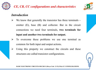
  • 1. BASIC ELECTRONIC CIRCUITS/19EC203/ E.Divya/ Unit 2/ CE,CB & CC CONFIGURATIONS CE, CB, CC configurations and characteristics Introduction  We know that generally the transistor has three terminals – emitter (E), base (B) and collector. But in the circuit connections we need four terminals, two terminals for input and another two terminals for output.  To overcome these problems we use one terminal as common for both input and output actions.  Using this property we construct the circuits and these structures are called transistor configurations.
  • 2. BASIC ELECTRONIC CIRCUITS/19EC203/ E.Divya/ Unit 2/ CE,CB & CC CONFIGURATIONS Generally there are three different configurations of transistors and they are common base (CB) configuration, common collector (CC) configuration and common emitter (CE) configuration. The behaviour of these three different configurations of transistors with respect to gain is given below. 1. Common Base (CB) Configuration: no current gain but voltage gain 2. Common Collector (CC) Configuration: current gain but no voltage gain 3. Common Emitter (CE) Configuration: current gain and voltage gain
  • 3. BASIC ELECTRONIC CIRCUITS/19EC203/ E.Divya/ Unit 2/ CE,CB & CC CONFIGURATIONS Common Base (CB) Configuration: In CB Configuration, the base terminal of the transistor will be connected common between the output and the input terminals.
  • 4. BASIC ELECTRONIC CIRCUITS/19EC203/ E.Divya/ Unit 2/ CE,CB & CC CONFIGURATIONS  The configuration name itself indicates the common terminal.  Here the input is applied between the base and emitter terminals and the corresponding output signal is taken between the base and collector terminals with the base terminal grounded.  Here the input parameters are VEB and IE and the output parameters are VCB and IC.  The input current flowing into the emitter terminal must be higher than the base current and collector current to operate the transistor, therefore the output collector current is less than the input emitter current.
  • 5. BASIC ELECTRONIC CIRCUITS/19EC203/ E.Divya/ Unit 2/ CE,CB & CC CONFIGURATIONS  The current gain is generally equal or less than to unity for this type of configuration.  This type of configuration has high resistance gain i.e. ratio of output resistance to input resistance is high.  The voltage gain for this configuration of circuit is given below. AV = Vout/Vin = (IC*RL) / (IE*Rin)  Current gain in common base configuration is given as α = Output current/Input current α = IC/IE
  • 6. BASIC ELECTRONIC CIRCUITS/19EC203/ E.Divya/ Unit 2/ CE,CB & CC CONFIGURATIONS Input Characteristics  Input characteristics are obtained between input current and input voltage with constant output voltage.  First keep the output voltage VCB constant and vary the input voltage VEB for different points then at each point record the input current IE value.  Repeat the same process at different output voltage levels.
  • 7. BASIC ELECTRONIC CIRCUITS/19EC203/ E.Divya/ Unit 2/ CE,CB & CC CONFIGURATIONS Output Characteristics  It is defined as the characteristic curve drawn between output voltage to output current whereas input current is constant.  To determine output characteristics, the emitter current IE is kept constant at zero and collector current Ic is increased from zero by increasing VCB.This is repeated for higher fixed values of IE.
  • 8. BASIC ELECTRONIC CIRCUITS/19EC203/ E.Divya/ Unit 2/ CE,CB & CC CONFIGURATIONS  In CB configuration a variation of the base-collector voltage results in a variation of the quasi- neutral width in the base.  The gradient of the minority-carrier density in the base therefore changes, yielding an increased collector current as the collector-base current is increased. This effect is referred to as the Early effect.