16 bit analog-to-digital converters for temperature sensors
•
0 recomendaciones•730 vistas

THIS IS PDF ABOUT 16 bit analog-to-digital converters for temperature sensors

Recomendados
Recomendados
Más contenido relacionado
Último
Último (20)
Destacado
Destacado (20)
16 bit analog-to-digital converters for temperature sensors
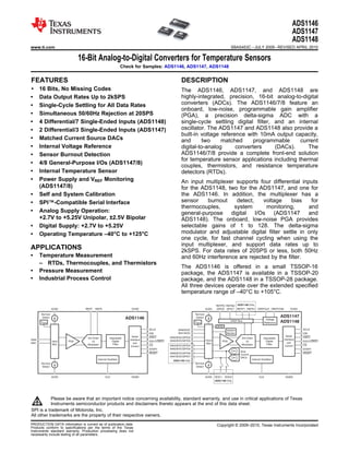
- 1. AD S1 148 ADS1146 AD S1 147 AD S1 146 ADS1147 ADS1148 www.ti.com SBAS453C – JULY 2009 – REVISED APRIL 2010 16-Bit Analog-to-Digital Converters for Temperature Sensors Check for Samples: ADS1146, ADS1147, ADS1148 1FEATURES DESCRIPTION • 23 16 Bits, No Missing Codes The ADS1146, ADS1147, and ADS1148 are • Data Output Rates Up to 2kSPS highly-integrated, precision, 16-bit analog-to-digital • Single-Cycle Settling for All Data Rates converters (ADCs). The ADS1146/7/8 feature an onboard, low-noise, programmable gain amplifier • Simultaneous 50/60Hz Rejection at 20SPS (PGA), a precision delta-sigma ADC with a • 4 Differential/7 Single-Ended Inputs (ADS1148) single-cycle settling digital filter, and an internal • 2 Differential/3 Single-Ended Inputs (ADS1147) oscillator. The ADS1147 and ADS1148 also provide a built-in voltage reference with 10mA output capacity, • Matched Current Source DACs and two matched programmable current • Internal Voltage Reference digital-to-analog converters (DACs). The • Sensor Burnout Detection ADS1146/7/8 provide a complete front-end solution for temperature sensor applications including thermal • 4/8 General-Purpose I/Os (ADS1147/8) couples, thermistors, and resistance temperature • Internal Temperature Sensor detectors (RTDs). • Power Supply and VREF Monitoring An input multiplexer supports four differential inputs (ADS1147/8) for the ADS1148, two for the ADS1147, and one for • Self and System Calibration the ADS1146. In addition, the multiplexer has a • SPI™-Compatible Serial Interface sensor burnout detect, voltage bias for thermocouples, system monitoring, and • Analog Supply Operation: general-purpose digital I/Os (ADS1147 and +2.7V to +5.25V Unipolar, ±2.5V Bipolar ADS1148). The onboard, low-noise PGA provides • Digital Supply: +2.7V to +5.25V selectable gains of 1 to 128. The delta-sigma • Operating Temperature –40°C to +125°C modulator and adjustable digital filter settle in only one cycle, for fast channel cycling when using the input multiplexer, and support data rates up to APPLICATIONS 2kSPS. For data rates of 20SPS or less, both 50Hz • Temperature Measurement and 60Hz interference are rejected by the filter. – RTDs, Thermocouples, and Thermistors The ADS1146 is offered in a small TSSOP-16 • Pressure Measurement package, the ADS1147 is available in a TSSOP-20 • Industrial Process Control package, and the ADS1148 in a TSSOP-28 package. All three devices operate over the extended specified temperature range of –40°C to +105°C. REFP0/ REFN0/ ADS1148 Only AVDD REFP REFN DVDD AVDD GPIO0 GPIO1 REFP1 REFN1 VREFOUT VREFCOM DVDD Burnout Burnout Detect ADS1146 Detect ADS1147 Voltage VBIAS VBIAS VREF Mux Reference ADS1148 GPIO SCLK AIN0/IEXC System SCLK DIN AIN1/IEXC Monitor DIN Serial DRDY Serial DRDY 3rd Order Adjustable AIN2/IEXC/GPIO2 3rd Order Adjustable AIN0 Interface Input Interface Input PGA DS Digital DOUT/DRDY AIN3/IEXC/GPIO3 PGA DS Digital DOUT/DRDY AIN1 and Mux and Mux Modulator Filter CS Modulator Filter CS Control AIN4/IEXC/GPIO4 Control START AIN5/IEXC/GPIO5 START Dual RESET AIN6/IEXC/GPIO6 RESET Current AIN7/IEXC/GPIO7 DACs Internal Oscillator Internal Oscillator ADS1148 Only Burnout Burnout Detect Detect AVSS CLK DGND AVSS IEXC1 IEXC2 CLK DGND ADS1148 Only 1 Please be aware that an important notice concerning availability, standard warranty, and use in critical applications of Texas Instruments semiconductor products and disclaimers thereto appears at the end of this data sheet. 2 SPI is a trademark of Motorola, Inc. 3 All other trademarks are the property of their respective owners. PRODUCTION DATA information is current as of publication date. Copyright © 2009–2010, Texas Instruments Incorporated Products conform to specifications per the terms of the Texas Instruments standard warranty. Production processing does not necessarily include testing of all parameters.
- 2. ADS1146 ADS1147 ADS1148 SBAS453C – JULY 2009 – REVISED APRIL 2010 www.ti.com This integrated circuit can be damaged by ESD. Texas Instruments recommends that all integrated circuits be handled with appropriate precautions. Failure to observe proper handling and installation procedures can cause damage. ESD damage can range from subtle performance degradation to complete device failure. Precision integrated circuits may be more susceptible to damage because very small parametric changes could cause the device not to meet its published specifications. PACKAGE/ORDERING INFORMATION (1) DUAL SENSOR EXCITATION NUMBER OF VOLTAGE CURRENT PACKAGE- PRODUCT RESOLUTION INPUTS REFERENCE SOURCES LEAD 1 Differential ADS1246 24 bits or External NO TSSOP-16 1 Single-Ended 2 Differential ADS1247 24 bits or Internal or External YES TSSOP-20 3 Single-Ended 4 Differential ADS1248 24 bits or Internal or External YES TSSOP-28 7 Single-Ended 1 Differential ADS1146 16 bits or External NO TSSOP-16 1 Single-Ended 2 Differential ADS1147 16 bits or Internal or External YES TSSOP-20 3 Single-Ended 4 Differential ADS1148 16 bits or Internal or External YES TSSOP-28 7 Single-Ended (1) For the most current package and ordering information, see the Package Option Addendum at the end of this document, or visit the device product folder on ti.com. ABSOLUTE MAXIMUM RATINGS (1) Over operating free-air temperature range, unless otherwise noted. ADS1146, ADS1147, ADS1148 UNIT AVDD to AVSS –0.3 to +5.5 V AVSS to DGND –2.8 to +0.3 V DVDD to DGND –0.3 to +5.5 V 100, momentary mA Input current 10, continuous mA Analog input voltage to AVSS AVSS – 0.3 to AVDD + 0.3 V Digital input voltage to DGND –0.3 to DVDD + 0.3 V Maximum junction temperature +150 °C Operating temperature range –40 to +125 °C Storage temperature range –60 to +150 °C (1) Stresses beyond those listed under Absolute Maximum Ratings may cause permanent damage to the device. These are stress ratings only, and functional operation of the device at these or any other conditions beyond those indicated is not implied. Exposure to absolute-maximum-rated conditions for extended periods may affect device reliability. 2 Submit Documentation Feedback Copyright © 2009–2010, Texas Instruments Incorporated Product Folder Link(s): ADS1146 ADS1147 ADS1148
- 3. ADS1146 ADS1147 ADS1148 www.ti.com SBAS453C – JULY 2009 – REVISED APRIL 2010 THERMAL INFORMATION ADS1146, ADS1147, ADS1148 THERMAL METRIC (1) UNITS PW 28 qJA Junction-to-ambient thermal resistance (2) 79.5 (3) qJC(top) Junction-to-case(top) thermal resistance 31.8 (4) qJB Junction-to-board thermal resistance 40.9 (5) °C/W yJT Junction-to-top characterization parameter 3.0 (6) yJB Junction-to-board characterization parameter 41.1 (7) qJC(bottom) Junction-to-case(bottom) thermal resistance n/a (1) For more information about traditional and new thermal metrics, see the IC Package Thermal Metrics application report, SPRA953. (2) The junction-to-ambient thermal resistance under natural convection is obtained in a simulation on a JEDEC-standard, high-K board, as specified in JESD51-7, in an environment described in JESD51-2a. (3) The junction-to-case (top) thermal resistance is obtained by simulating a cold plate test on the package top. No specific JEDEC-standard test exists, but a close description can be found in the ANSI SEMI standard G30-88. (4) The junction-to-board thermal resistance is obtained by simulating in an environment with a ring cold plate fixture to control the PCB temperature, as described in JESD51-8. (5) The junction-to-top characterization parameter, yJT, estimates the junction temperature of a device in a real system and is extracted from the simulation data for obtaining qJA, using a procedure described in JESD51-2a (sections 6 and 7). (6) The junction-to-board characterization parameter, yJB, estimates the junction temperature of a device in a real system and is extracted from the simulation data for obtaining qJA , using a procedure described in JESD51-2a (sections 6 and 7). (7) The junction-to-case (bottom) thermal resistance is obtained by simulating a cold plate test on the exposed (power) pad. No specific JEDEC standard test exists, but a close description can be found in the ANSI SEMI standard G30-88. Copyright © 2009–2010, Texas Instruments Incorporated Submit Documentation Feedback 3 Product Folder Link(s): ADS1146 ADS1147 ADS1148
- 4. ADS1146 ADS1147 ADS1148 SBAS453C – JULY 2009 – REVISED APRIL 2010 www.ti.com ELECTRICAL CHARACTERISTICS Minimum/maximum specifications apply from –40°C to +105°C. Typical specifications are at +25°C. All specifications at AVDD = +5V, DVDD = +3.3V, AVSS = DGND = 0V, VREF = +2.048V, and oscillator frequency = 4.096MHz, unless otherwise noted. ADS1146, ADS1147, ADS1148 PARAMETER CONDITIONS MIN TYP MAX UNIT ANALOG INPUTS Full-scale input voltage ±VREF/PGA 2.7/PGA V (VIN = ADCINP – ADCINN) (VIN)(Gain) (VIN)(Gain) Common-mode input range AVSS + 0.1V + AVDD - 0.1V - V 2 2 Differential input current 100 pA 1, 2, 4, 8, 16, 32, PGA gain settings 64, 128 Burnout current source 0.5, 2, or 10 mA Bias voltage (AVDD + AVSS)/2 V Bias voltage output impedance 400 Ω pA Mux leakage current pA SYSTEM PERFORMANCE Resolution No missing codes 16 Bits 5, 10, 20, 40, 80, Data rate 160, 320, 640, SPS 1000, 2000 Integral nonlinearity (INL) Differential input, end point fit, PGA = 1 ±0.5 ±1 LSB Offset error After calibration 1 LSB PGA = 1 100 nV/°C Offset drift PGA = 128 15 nV/°C Gain error Excluding VREF errors ±0.5 % PGA = 1, excludes VREF drift 1 ppm/°C Gain drift PGA = 128, excludes VREF drift –3.5 ppm/°C ADC conversion time Single-cycle settling See Table 15 Noise See Table 5 and Table 6 Normal-mode rejection See Table 8 At dc, PGA = 1 90 dB Common-mode rejection At dc, PGA = 32 100 dB Power-supply rejection AVDD, DVDD at dc 100 dB VOLTAGE REFERENCE INPUT Voltage reference input (AVDD – AVSS) 0.5 V (VREF = VREFP – VREFN) –1 Negative reference input (REFN) AVSS – 0.1 REFP – 0.5 V Positive reference input (REFP) REFN + 0.5 AVDD + 0.1 V Reference input current 30 nA ON-CHIP VOLTAGE REFERENCE Output voltage 2.038 2.048 2.058 V Output current (1) ±10 mA Load regulation 50 mV/mA Drift (2) TA = –40°C to +105°C 20 50 ppm/°C Startup time See Table 9 ms (1) Do not exceed this loading on the internal voltage reference. (2) Specified by the combination of design and final production test. 4 Submit Documentation Feedback Copyright © 2009–2010, Texas Instruments Incorporated Product Folder Link(s): ADS1146 ADS1147 ADS1148
- 5. ADS1146 ADS1147 ADS1148 www.ti.com SBAS453C – JULY 2009 – REVISED APRIL 2010 ELECTRICAL CHARACTERISTICS (continued) Minimum/maximum specifications apply from –40°C to +105°C. Typical specifications are at +25°C. All specifications at AVDD = +5V, DVDD = +3.3V, AVSS = DGND = 0V, VREF = +2.048V, and oscillator frequency = 4.096MHz, unless otherwise noted. ADS1146, ADS1147, ADS1148 PARAMETER CONDITIONS MIN TYP MAX UNIT CURRENT SOURCES (IDACS) 50, 100, 250, Output current 500, 750, 1000, mA 1500 Voltage compliance All currents AVDD – 0.7 V Initial error All currents, each IDAC –6 ±1.0 6 % of FS Initial mismatch All currents, between IDACs ±0.03 % of FS Temperature drift Each IDAC 200 ppm/°C Temperature drift matching Between IDACs 10 ppm/°C SYSTEM MONITORS Temperature Voltage TA = +25°C 118 mV sensor reading Drift 405 mV/°C GENERAL-PURPOSE INPUT/OUTPUT (GPIO) VIH 0.7AVDD AVDD V VIL AVSS 0.3AVDD V Logic levels VOH IOH = 1mA 0.8AVDD V VOL IOL = 1mA AVSS 0.2 AVDD V DIGITAL INPUT/OUTPUT (other than GPIO) VIH 0.7DVDD DVDD V VIL DGND 0.3DVDD V Logic levels VOH IOH = 1mA 0.8DVDD V VOL IOL = 1mA DGND 0.2 DVDD V Input leakage DGND < VDIGITAL IN < DVDD ±10 mA Clock input Frequency 1 4.5 MHz (CLK) Duty cycle 25 75 % Internal oscillator frequency 3.89 4.096 4.3 MHz POWER SUPPLY DVDD 2.7 5.25 V AVSS –2.5 0 V AVDD AVSS + 2.7 AVSS + 5.25 V Normal mode, DVDD = 5V, 230 mA data rate = 20SPS, internal oscillator DVDD current Normal mode, DVDD = 3.3V, 210 mA data rate = 20SPS, internal oscillator Sleep mode 0.2 µA Converting, AVDD = 5V, 225 µA data rate = 20SPS, external reference Converting, AVDD = 3.3V, 212 µA AVDD current data rate = 20SPS, external reference Sleep mode 0.1 µA Additional current with internal reference 180 mA enabled AVDD = DVDD = 5V, data rate = 20SPS, 2.3 mW external reference, internal oscillator Power dissipation AVDD = DVDD = 3.3V, data rate = 20SPS, 1.4 mW external reference, internal oscillator TEMPERATURE RANGE Specified –40 +105 °C Operating –40 +125 °C Storage –60 +150 °C Copyright © 2009–2010, Texas Instruments Incorporated Submit Documentation Feedback 5 Product Folder Link(s): ADS1146 ADS1147 ADS1148
- 6. ADS1146 ADS1147 ADS1148 SBAS453C – JULY 2009 – REVISED APRIL 2010 www.ti.com PIN CONFIGURATIONS PW PACKAGE TSSOP-28 (TOP VIEW) DVDD 1 28 SCLK DGND 2 27 DIN CLK 3 26 DOUT/DRDY RESET 4 25 DRDY REFP0/GPIO0 5 24 CS REFN0/GPIO1 6 23 START REFP1 7 22 AVDD ADS1148 REFN1 8 21 AVSS VREFOUT 9 20 IEXC1 VREFCOM 10 19 IEXC2 AIN0/IEXC 11 18 AIN3/IEXC/GPIO3 AIN1/IEXC 12 17 AIN2/IEXC/GPIO2 AIN4/IEXC/GPIO4 13 16 AIN7/IEXC/GPIO7 AIN5/IEXC/GPIO5 14 15 AIN6/IEXC/GPIO6 6 Submit Documentation Feedback Copyright © 2009–2010, Texas Instruments Incorporated Product Folder Link(s): ADS1146 ADS1147 ADS1148
- 7. ADS1146 ADS1147 ADS1148 www.ti.com SBAS453C – JULY 2009 – REVISED APRIL 2010 ADS1148 (TSSOP-28) PIN DESCRIPTIONS NAME PIN NO. FUNCTION DESCRIPTION DVDD 1 Digital Digital power supply DGND 2 Digital Digital ground CLK 3 Digital input External clock input. Tie this pin to DGND to activate the internal oscillator. RESET 4 Digital input Chip reset (active low). Returns all register values to reset values. Analog input Positive external reference input 0, or REFP0/GPIO0 5 Digital in/out general-purpose digital input/output pin 0 Analog input Negative external reference 0 input, or REFN0/GPIO1 6 Digital in/out general-purpose digital input/output pin 1 REFP1 7 Analog input Positive external reference 1 input REFN1 8 Analog input Negative external reference 1 input VREFOUT 9 Analog output Positive internal reference voltage output Negative internal reference voltage output. Connect this pin to AVSS when using a unipolar VREFCOM 10 Analog output supply, or to the midvoltage of the power supply when using a bipolar supply. AIN0/IEXC 11 Analog input Analog input 0, optional excitation current output AIN1/IEXC 12 Analog input Analog input 1, optional excitation current output Analog input Analog input 4, optional excitation current output, or AIN4/IEXC/GPIO4 13 Digital in/out general-purpose digital input/output pin 4 Analog input Analog input 5, optional excitation current output, or AIN5/IEXC/GPIO5 14 Digital in/out general-purpose digital input/output pin 5 Analog input Analog input 6, optional excitation current output, or AIN6/IEXC/GPIO6 15 Digital in/out general-purpose digital input/output pin 6 Analog input Analog input 7, optional excitation current output, or AIN7/IEXC/GPIO7 16 Digital in/out general-purpose digital input/output pin 7 Analog input Analog input 2, optional excitation current output, or AIN2/IEXC/GPIO2 17 Digital in/out general-purpose digital input/output pin 2 Analog input Analog input 3, optional excitation current output, or AIN3/IEXC/GPIO3 18 Digital in/out general-purpose digital input/output pin 3 IEXC2 19 Analog output Excitation current output 2 IEXC1 20 Analog output Excitation current output 1 AVSS 21 Analog Negative analog power supply AVDD 22 Analog Positive analog power supply START 23 Digital input Conversion start. See text for complete description. CS 24 Digital input Chip select (active low) DRDY 25 Digital output Data ready (active low) Serial data out output, or DOUT/DRDY 26 Digital output data out combined with data ready (active low when DRDY function enabled) DIN 27 Digital input Serial data input SCLK 28 Digital input Serial clock input Copyright © 2009–2010, Texas Instruments Incorporated Submit Documentation Feedback 7 Product Folder Link(s): ADS1146 ADS1147 ADS1148
- 8. ADS1146 ADS1147 ADS1148 SBAS453C – JULY 2009 – REVISED APRIL 2010 www.ti.com PW PACKAGE TSSOP-20 (TOP VIEW) DVDD 1 20 SCLK DGND 2 19 DIN CLK 3 18 DOUT/DRDY RESET 4 17 DRDY REFP0/GPIO0 5 16 CS ADS1147 REFN0/GPIO1 6 15 START VREFOUT 7 14 AVDD VREFCOM 8 13 AVSS AIN0/IEXC 9 12 AIN3/IEXC/GPIO3 AIN1/IEXC 10 11 AIN2/IEXC/GPIO2 ADS1147 (TSSOP-20) PIN DESCRIPTIONS NAME PIN NO. FUNCTION DESCRIPTION DVDD 1 Digital Digital power supply DGND 2 Digital Digital ground CLK 3 Digital input External clock input. Tie this pin to DGND to activate the internal oscillator. RESET 4 Digital input Chip reset (active low). Returns all register values to reset values. Analog input Positive external reference input, or REFP0/GPIO0 5 Digital in/out general-purpose digital input/output pin 0 Analog input Negative external reference input, or REFN0/GPIO1 6 Digital in/out general-purpose digital input/output pin 1 VREFOUT 7 Analog output Positive internal reference voltage output Negative internal reference voltage output. Connect this pin to AVSS when using a unipolar VREFCOM 8 Analog output supply, or to the midvoltage of the power supply when using a bipolar supply. AIN0/IEXC 9 Analog input Analog input 0, optional excitation current output AIN1/IEXC 10 Analog input Analog input 1, optional excitation current output Analog input Analog input 2, optional excitation current output, or AIN2/IEXC/GPIO2 11 Digital in/out general-purpose digital input/output pin 2 Analog input Analog input 3, with or without excitation current output, or AIN3/IEXC/GPIO3 12 Digital in/out general-purpose digital input/output pin 3 AVSS 13 Analog Negative analog power supply AVDD 14 Analog Positive analog power supply START 15 Digital input Conversion start. See text for description of use. CS 16 Digital input Chip select (active low) DRDY 17 Digital output Data ready (active low) Serial data out output, or DOUT/DRDY 18 Digital output data out combined with data ready (active low when DRDY function enabled) DIN 19 Digital input Serial data input SCLK 20 Digital input Serial clock input 8 Submit Documentation Feedback Copyright © 2009–2010, Texas Instruments Incorporated Product Folder Link(s): ADS1146 ADS1147 ADS1148
- 9. ADS1146 ADS1147 ADS1148 www.ti.com SBAS453C – JULY 2009 – REVISED APRIL 2010 PW PACKAGE TSSOP-16 (TOP VIEW) DVDD 1 16 SCLK DGND 2 15 DIN CLK 3 14 DOUT/DRDY RESET 4 13 DRDY ADS1146 REFP 5 12 CS REFN 6 11 START AINP 7 10 AVDD AINN 8 9 AVSS ADS1146 (TSSOP-16) PIN DESCRIPTIONS NAME PIN NO. FUNCTION DESCRIPTION DVDD 1 Digital Digital power supply DGND 2 Digital Digital ground CLK 3 Digital input External clock input. Tie this pin to DGND to activate the internal oscillator. RESET 4 Digital input Chip reset (active low). Returns all register values to reset values. REFP 5 Analog input Positive external reference input REFN 6 Analog input Negative external reference input AINP 7 Analog input Positive analog input AINN 8 Analog input Negative analog input AVSS 9 Analog Negative analog power supply AVDD 10 Analog Positive analog power supply START 11 Digital input Conversion start. See text for description of use. CS 12 Digital input Chip select (active low) DRDY 13 Digital output Data ready (active low) Serial data out output, or DOUT/DRDY 14 Digital output data out combined with data ready (active low when DRDY function enabled) DIN 15 Digital input Serial data input SCLK 16 Digital input Serial clock input Copyright © 2009–2010, Texas Instruments Incorporated Submit Documentation Feedback 9 Product Folder Link(s): ADS1146 ADS1147 ADS1148
- 10. ADS1146 ADS1147 ADS1148 SBAS453C – JULY 2009 – REVISED APRIL 2010 www.ti.com TIMING DIAGRAMS CS tSPWH tCSSC tSCLK tSCCS SCLK tDIST tDIHD tSPWL DIN DIN[0] DIN[7] DIN[6] DIN[5] DIN[4] DIN[1] DIN[0] tDOPD tDOHD (1) DOUT[7] DOUT[6] DOUT[5] DOUT[4] DOUT[1] DOUT[0] DOUT/DRDY tCSDO Figure 1. Serial Interface Timing (1) Table 1. Timing Characteristics for Figure 1 SYMBOL DESCRIPTION MIN MAX UNIT tCSSC CS low to first SCLK high (set up time) 10 ns (2) tSCCS SCLK low to CS high (hold time) 7 tOSC tDIST DIN set up time 5 ns tDIHD DIN hold time 5 ns tDOPD SCLK rising edge to new data valid 30 ns tDOHD DOUT hold time 0 ns 500 ns tSCLK SCLK period 64 conversions tSPWH SCLK pulse width high 0.25 0.75 tSCLK tSPWL SCLK pulse width low 0.25 0.75 tSCLK tCSDO CS high to DOUT high impedance 10 ns (1) DRDY MODE bit = 0. (2) tOSC = 1/fCLK. The default clock frequency fCLK = 4.096MHz. tDTS tPWH DRDY tSTD 1 2 3 4 5 6 7 8 SCLK(3) Figure 2. SPI Interface Timing to Allow Conversion Result Loading (3) (4) Table 2. Timing Characteristics for Figure 2 SYMBOL DESCRIPTION MIN MAX UNIT tPWH DRDY pulse width high 3 tOSC tS TD SCLK low prior to DRDY low 5 tOSC tDTS DRDY falling edge to SCLK rising edge 30 ns (3) This timing diagram is applicable only when the CS pin is low. SCLK need not be low during tSTD when CS is high. (4) SCLK should only be sent in multiples of eight during partial retrieval of output data. 10 Submit Documentation Feedback Copyright © 2009–2010, Texas Instruments Incorporated Product Folder Link(s): ADS1146 ADS1147 ADS1148
- 11. ADS1146 ADS1147 ADS1148 www.ti.com SBAS453C – JULY 2009 – REVISED APRIL 2010 START tSTART Figure 3. Minimum START Pulse Width Table 3. Timing Characteristics for Figure 3 SYMBOL DESCRIPTION MIN MAX UNIT tSTART START pulse width high 3 tOSC tRESET RESET CS SCLK tRHSC Figure 4. Reset Pulse Width and SPI Communication After Reset Table 4. Timing Characteristics for Figure 4 SYMBOL DESCRIPTION MIN MAX UNIT t RESET RESET pulse width low 4 tOSC tRHSC RESET high to SPI communication start 0.6 (1) ms (1) For fOSC = 4.096MHz, scales proportionately with fOSC frequency. Copyright © 2009–2010, Texas Instruments Incorporated Submit Documentation Feedback 11 Product Folder Link(s): ADS1146 ADS1147 ADS1148
- 12. ADS1146 ADS1147 ADS1148 SBAS453C – JULY 2009 – REVISED APRIL 2010 www.ti.com NOISE PERFORMANCE The ADS1146/7/8 noise performance can be optimized by adjusting the data rate and PGA setting. As the averaging is increased by reducing the data rate, the noise drops correspondingly. Increasing the PGA value reduces the input-referred noise, particularly useful when measuring low-level signals. Table 5 and Table 6 summarize noise performance of the ADS1146/7/8. The data are representative of typical noise performance at T = +25°C. The data shown are the result of averaging the readings from multiple devices and were measured with the inputs shorted together. Table 5 lists the input-referred noise in units mVPP. In many of the settings, especially at lower data rates, the inherent device noise is less than 1LSB. For these cases, the noise is rounded up to 1LSB. Table 6 lists the corresponding data in units of ENOB (effective number of bits) where: ENOB = ln(Full-Scale Range/Noise)/ln(2) (1) Table 5. Noise in mVPP At VREF = 2.048V, AVDD = 5V, and AVSS = 0V PGA SETTING DATA RATE (SPS) 1 2 4 8 16 32 64 128 (1) (1) (1) (1) (1) (1) (1) 5 62.50 31.25 15.63 7.81 3.91 1.95 0.98 0.49 (1) (1) (1) (1) (1) (1) (1) (1) 10 62.50 31.25 15.63 7.81 3.91 1.95 0.98 0.49 (1) (1) (1) (1) (1) (1) (1) (1) 20 62.50 31.25 15.63 7.81 3.91 1.95 0.98 0.55 40 62.50 (1) 31.25 (1) 15.63 (1) 7.81 (1) 3.91 (1) 1.95 (1) 0.98 (1) 0.75 (1) (1) (1) (1) (1) (1) 80 62.50 31.25 15.63 7.81 3.91 1.95 1.09 0.98 160 62.50 (1) 31.25 (1) 15.63 (1) 7.81 (1) 3.91 (1) 1.95 (1) 1.88 1.57 320 62.50 (1) 35.30 17.52 8.86 4.35 3.03 2.44 2.34 640 93.06 45.20 18.73 12.97 6.51 4.20 3.69 3.50 1000 284.59 129.77 61.30 33.04 16.82 9.08 5.42 4.65 2000 273.39 130.68 67.13 36.16 19.22 9.87 6.93 6.48 (1) Peak-to-peak noise rounded up to 1LSB. Table 6. Effective Number of Bits From Peak-to-Peak Noise At VREF = 2.048V, AVDD = 5V, and AVSS = 0V PGA SETTING DATA RATE (SPS) 1 2 4 8 16 32 64 128 5 16 16 16 16 16 16 16 16 10 16 16 16 16 16 16 16 16 20 16 16 16 16 16 16 16 15.8 40 16 16 16 16 16 16 16 15.4 80 16 16 16 16 16 16 15.8 15.0 160 16 16 16 16 16 16 15.1 14.3 320 16 15.8 15.8 15.8 15.8 15.4 14.7 13.7 640 15.4 15.5 15.7 15.3 15.3 14.9 14.1 13.2 1000 13.8 13.9 14.0 13.9 13.9 13.8 13.5 12.7 2000 13.9 13.9 13.9 13.8 13.7 13.7 13.2 12.3 12 Submit Documentation Feedback Copyright © 2009–2010, Texas Instruments Incorporated Product Folder Link(s): ADS1146 ADS1147 ADS1148
- 13. ADS1146 ADS1147 ADS1148 www.ti.com SBAS453C – JULY 2009 – REVISED APRIL 2010 TYPICAL CHARACTERISTICS At TA = +25°C, AVDD = 5V, VREF = 2.5V, and AVSS = 0V, unless otherwise noted. ANALOG CURRENT DIGITAL CURRENT vs TEMPERATURE vs TEMPERATURE 800 330 2kSPS DVDD = 5V 700 310 2kSPS 600 Analog Current (mA) 290 Digital Current (mA) 320/640/1kSPS 500 320/640/1kSPS 40/80/160SPS 270 400 5/10/20SPS 250 300 230 200 40/80/160SPS 100 210 5/10/20SPS 0 190 -40 -20 0 20 40 60 80 100 120 -40 -20 0 20 40 60 80 100 120 Temperature (°C) Temperature (°C) Figure 5. Figure 6. IDAC LINE REGULATION IDAC DRIFT 1.002 0.004 1.5mA Setting, 10 Units 1.001 0.003 1.000 Normalized Output Current 0.999 0.002 IEXC1 - IEXC2 (mA) 50mA 0.998 100mA 0.001 0.997 500mA 0 0.996 250mA 0.995 750mA -0.001 0.994 -0.002 IDAC Current Settings 0.993 1mA -0.003 0.992 1.5mA 0.991 -0.004 2.0 2.5 3.0 3.5 4.0 4.5 5.0 5.5 6.0 -40 -20 0 20 40 60 80 100 120 AVDD (V) Temperature (°C) Figure 7. Figure 8. Copyright © 2009–2010, Texas Instruments Incorporated Submit Documentation Feedback 13 Product Folder Link(s): ADS1146 ADS1147 ADS1148
- 14. ADS1146 ADS1147 ADS1148 SBAS453C – JULY 2009 – REVISED APRIL 2010 www.ti.com GENERAL DESCRIPTION OVERVIEW The ADS1147 and ADS1148 also include a flexible The ADS1146, ADS1147 and ADS1148 are highly input multiplexer with system monitoring capability integrated 24-bit data converters. Each device and general-purpose I/O settings, a very low-drift includes a low-noise, high-impedance programmable voltage reference, and two matched current sources gain amplifier (PGA), a delta-sigma (ΔΣ) ADC with an for sensor excitation. Figure 9 and Figure 10 show adjustable single-cycle settling digital filter, internal the various functions incorporated into each device. oscillator, and a simple but flexible SPI-compatible serial interface. AVDD REFP REFN DVDD Burnout Detect ADS1146 VBIAS SCLK DIN Serial DRDY 3rd Order Adjustable AIN0 Interface Input PGA DS Digital DOUT/DRDY AIN1 and Mux Modulator Filter CS Control START RESET Internal Oscillator Burnout Detect AVSS CLK DGND Figure 9. ADS1146 Diagram REFP0/ REFN0/ ADS1148 Only AVDD GPIO0 GPIO1 REFP1 REFN1 VREFOUT VREFCOM DVDD Burnout Detect ADS1147 Voltage VBIAS VREF Mux ADS1148 Reference GPIO AIN0/IEXC System SCLK AIN1/IEXC Monitor DIN Serial DRDY AIN2/IEXC/GPIO2 3rd Order Adjustable Input Interface AIN3/IEXC/GPIO3 PGA DS Digital DOUT/DRDY Mux and Modulator Filter CS AIN4/IEXC/GPIO4 Control AIN5/IEXC/GPIO5 START Dual AIN6/IEXC/GPIO6 RESET Current AIN7/IEXC/GPIO7 DACs Internal Oscillator ADS1148 Only Burnout Detect AVSS IEXC1 IEXC2 CLK DGND ADS1148 Only Figure 10. ADS1147, ADS1148 Diagram 14 Submit Documentation Feedback Copyright © 2009–2010, Texas Instruments Incorporated Product Folder Link(s): ADS1146 ADS1147 ADS1148
- 15. ADS1146 ADS1147 ADS1148 www.ti.com SBAS453C – JULY 2009 – REVISED APRIL 2010 ADC INPUT AND MULTIPLEXER Any analog input pin can be selected as the positive input or negative input through the MUX0 register. The ADS1146/7/8 ADC measures the input signal The ADS1146/7/8 have a true fully differential mode, through the onboard PGA. All analog inputs are meaning that the input signal range can be from connected to the internal AINP or AINN analog inputs –2.5V to +2.5V (when AVDD = 2.5V and AVSS = through the analog multiplexer. A block diagram of –2.5V). the analog input multiplexer is shown in Figure 11. Through the input multiplexer, the ambient The input multiplexer connects to eight (ADS1148), temperature (internal temperature sensor), AVDD, four (ADS1147), or two (ADS1146) analog inputs that DVDD, and external reference can all be selected for can be configured as single-ended inputs, differential measurement. Refer to the System Monitor section inputs, or in a combination of single-ended and for details. differential inputs. The multiplexer also allows the on-chip excitation current and/or bias voltage to be On the ADS1147 and ADS1148, the analog inputs selected to a specific channel. can also be configured as general-purpose inputs/outputs (GPIOs). See the General-Purpose Digital I/O section for more details. AVDD AVDD IDAC2 IDAC1 System Monitors AVSS AVDD VBIAS AVDD AVDD AIN0 AVSS AVDD VBIAS Temperature VREFP Diode VREFN AIN1 ADS1147/8 Only VREFP1/4 AVSS AVDD VBIAS VREFN1/4 AIN2 VREFP0/4 VREFN0/4 AVSS AVDD VBIAS AVDD/4 AIN3 AVSS/4 DVDD/4 ADS1148 Only DGND/4 AVSS AVDD VBIAS AIN4 AVDD AVSS AVDD VBIAS Burnout Current Source (0.5mA, 2mA, 10mA) AIN5 AINP To VBIAS PGA AVSS AVDD AINN ADC AIN6 Burnout Current Source AVSS AVDD VBIAS (0.5mA, 2mA, 10mA) AIN7 AVSS Figure 11. Analog Input Multiplexer Circuit Copyright © 2009–2010, Texas Instruments Incorporated Submit Documentation Feedback 15 Product Folder Link(s): ADS1146 ADS1147 ADS1148
- 16. ADS1146 ADS1147 ADS1148 SBAS453C – JULY 2009 – REVISED APRIL 2010 www.ti.com ESD diodes protect the ADC inputs. To prevent these As with the analog inputs, REFP0 and REFN0 can be diodes from turning on, make sure the voltages on configured as digital I/Os on the ADS1147 and the input pins do not go below AVSS by more than ADS1148. 100mV, and do not exceed AVDD by more than 100mV, as shown in Equation 2. Note that the same ADS1148 Only caution is true if the inputs are configured to be REFP1 REFN1 REFP0 REFN0 VREFOUT VREFCOM GPIOs. AVSS – 100mV < (AINX) < AVDD + 100mV (2) Settling Time for Channel Multiplexing Internal The ADS1146/7/8 is a true single-cycle settling ΔΣ Reference Multiplexer Voltage converter. The first data available after the start of a Reference conversion are fully settled and valid for use. The VREFP VREFN time required to settle is roughly equal to the inverse of the data rate. The exact time depends on the ADC specific data rate and the operation that resulted in the start of a conversion; see Table 15 for specific values. Figure 12. Reference Input Multiplexer VOLTAGE REFERENCE INPUT The voltage reference for the ADS1146/7/8 is the The reference input circuit has ESD diodes to protect differential voltage between REFP and REFN: the inputs. To prevent the diodes from turning on, make sure the voltage on the reference input pin is VREF = VREFP – VREFN not less than AVSS – 100mV, and does not exceed In the case of the ADS1146, these pins are dedicated AVDD + 100mV, as shown in Equation 3: inputs. For the ADS1147 and ADS1148, there is a AVSS – 100mV < (VREFP or VREFN) < AVDD + 100mV (3) multiplexer that selects the reference inputs, as shown in Figure 12. The reference input uses a buffer to increase the input impedance. 16 Submit Documentation Feedback Copyright © 2009–2010, Texas Instruments Incorporated Product Folder Link(s): ADS1146 ADS1147 ADS1148
- 17. ADS1146 ADS1147 ADS1148 www.ti.com SBAS453C – JULY 2009 – REVISED APRIL 2010 LOW-NOISE PGA (AVSS + 0.1V + (VIN)(Gain) 2 ) ( (V )(Gain) £ VCMI £ AVDD - 0.1V - IN 2 ) The ADS1146/7/8 feature a low-drift, low-noise, high (4) input impedance programmable gain amplifier (PGA). The PGA can be set to gain of 1, 2, 4, 8, 16, 32, 64, or 128 by register SYS0. A simplified diagram of the MODULATOR PGA is shown in Figure 13. A third-order modulator is used in the ADS1146/7/8. The modulator converts the analog input voltage into 454W a pulse code modulated (PCM) data stream. To save AINP power, the modulator clock runs from 32kHz up to 7.5pF A1 512kHz for different data rates, as shown in Table 7. R DIGITAL FILTER 7.5pF The ADS1146/7/8 use linear-phase finite impulse R C ADC response (FIR) digital filters that can be adjusted for different output data rates. The digital filter always settles in a single cycle. 7.5pF Table 8 shows the exact data rates when an external 454W A2 oscillator equal to 4.096MHz is used. Also shown is AINN the signal –3dB bandwidth, and the 50Hz and 60Hz 7.5pF attenuation. For good 50Hz or 60Hz rejection, use a data rate of 20SPS or slower. The frequency responses of the digital filter are Figure 13. Simplified Diagram of the PGA shown in Figure 14 to Figure 24. Figure 17 shows a detailed view of the filter frequency response from The PGA consists of two chopper-stabilized 48Hz to 62Hz for a 20SPS data rate. All filter plots amplifiers (A1 and A2) and a resistor feedback are generated with 4.096MHz external clock. network that sets the gain of the PGA. The PGA input is equipped with an electromagnetic interference Table 7. Modulator Clock Frequency for Different (EMI) filter, as shown in Figure 13. Note that as with Data Rates any PGA, it is necessary to ensure that the input DATA RATE fMOD voltage stays within the specified common-mode (SPS) (kHz) input range specified in the Electrical Characteristics. 5, 10, 20 32 The common-mode input (VCMI) must be within the 40, 80, 160 128 range shown in Equation 4: 320, 640, 1000 256 2000 512 Table 8. Digital Filter Specifications (1) ATTENUATION DATA RATE –3dB BANDWIDTH fIN = 50Hz ±0.3Hz fIN = 60Hz ±0.3Hz fIN = 50Hz ±1Hz fIN = 60Hz ±1Hz 5SPS 2.26Hz –106dB –74dB –81dB –69dB 10SPS 4.76Hz –106dB –74dB –80dB –69dB 20SPS 14.8Hz –71dB –74dB –66dB –68dB 40SPS 9.03Hz 80SPS 19.8Hz 160SPS 118Hz 320SPS 154Hz 640SPS 495Hz 1000SPS 732Hz 2000SPS 1465Hz (1) Values shown for fOSC = 4.096MHz. Copyright © 2009–2010, Texas Instruments Incorporated Submit Documentation Feedback 17 Product Folder Link(s): ADS1146 ADS1147 ADS1148