1. 1 CAUTION: These devices are sensitive to electrostatic discharge; follow proper IC Handling Procedures.
1-888-INTERSIL or 1-888-468-3774 |Copyright Intersil Americas Inc. 2007, 2011. All Rights Reserved
Intersil (and design) is a trademark owned by Intersil Corporation or one of its subsidiaries.
All other trademarks mentioned are the property of their respective owners.
Application Note 1325
Authors: Tamara Schmitz and Mike Wong
Choosing and Using Bypass Capacitors
Introduction
Bypass capacitors are found in every working piece of
electronic equipment. Most engineers know that systems,
circuits, and individual chips need to be bypassed. The
methods for choosing bypass capacitors typically follow
decisions of tradition instead of optimizing for any particular
circuit. This application note aims to bring the design aspect
back to this seemingly simple component. After discussing the
motivation for using bypass caps, we form a vocabulary around
the basics; equivalent circuit, dielectrics and types of available
capacitors.
The next step is identifying the primary function and
environment of the bypass capacitor. Circuits that exhibit large
current spikes have different bypassing needs than ones that
solely operate at high frequencies. A few special options are
discussed, like scaling multiple bypass capacitors, as well as
the importance of board layout.
Finally, we present four application examples. These represent
circuits with high and low currents as well as those with high
and low frequencies.
Motivation
It’s far too common (and quite distressing) to breadboard a
circuit in an ideal configuration; only to find that it doesn’t work
well or it doesn’t work at all (Figure 1). Noise may have coupled
into the circuit from the power supply, internal IC circuitry, or
nearby IC. Wires and board connections act like antennas and
power supply levels change with current draw.
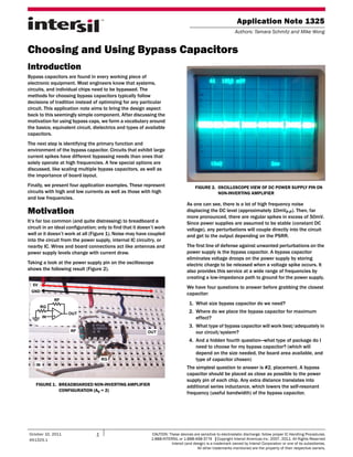
Taking a look at the power supply pin on the oscilloscope
shows the following result (Figure 2).
.
As one can see, there is a lot of high frequency noise
displacing the DC level (approximately 10mVP-P). Then, far
more pronounced, there are regular spikes in excess of 50mV.
Since power supplies are assumed to be stable (constant DC
voltage), any perturbations will couple directly into the circuit
and get to the output depending on the PSRR.
The first line of defense against unwanted perturbations on the
power supply is the bypass capacitor. A bypass capacitor
eliminates voltage droops on the power supply by storing
electric charge to be released when a voltage spike occurs. It
also provides this service at a wide range of frequencies by
creating a low-impedance path to ground for the power supply.
We have four questions to answer before grabbing the closest
capacitor:
1. What size bypass capacitor do we need?
2. Where do we place the bypass capacitor for maximum
effect?
3. What type of bypass capacitor will work best/adequately in
our circuit/system?
4. And a hidden fourth question—what type of package do I
need to choose for my bypass capacitor? (which will
depend on the size needed, the board area available, and
type of capacitor chosen)
The simplest question to answer is #2, placement. A bypass
capacitor should be placed as close as possible to the power
supply pin of each chip. Any extra distance translates into
additional series inductance, which lowers the self-resonant
frequency (useful bandwidth) of the bypass capacitor.
FIGURE 1. BREADBOARDED NON-INVERTING AMPLIFIER
CONFIGURATION (AV = 2)
5V
GND
RF
RG
OUT
IN
OUT
IN
RF
RG
+
-
FIGURE 2. OSCILLOSCOPE VIEW OF DC POWER SUPPLY PIN ON
NON-INVERTING AMPLIFIER
October 10, 2011
AN1325.1
2. Application Note 1325
2 AN1325.1
October 10, 2011
The effect of the bypass capacitor on the output of the
non-inverting amplifier can be seen in Figure 4.
Further improvements in dealing with the placement and routing
of the bypass capacitor will involve discussion of printed circuit
board design—the topic of our next in-depth discussion.
The other three questions (about capacitor size, type, and
package choice) are the heart of this discussion. These topics will
be discussed in detail after first reviewing capacitor basics.
Capacitor Basics
The classic definition of a capacitor is two conductive plates
separated by a dielectric material. As charge collects on the
plates, an electric field builds across the dielectric. The amount
of charge needed to create a certain potential between the
plates is referred to as capacitance and is measured in Farads.
The capacitance can also be measured by the dimensions of the
plates and quality of the dielectric (Figure 5, Equation 1).
Capacitance increases as the area of the plates increases since
more charge can be stored as the potential is created. The
distance between the plates dictates the attraction between
charges stored on them. As the distance increases, the
interaction is decreased, and therefore so is the capacitance.
This discussion also relates the relationship shown in Figure 5,
Equation 2.
The last of the basic equations involves current. By definition,
current is the movement of charge (Figure 5, Equation 3).
Therefore, there can only be movement of charge when the
voltage (potential between the plates) is changing. In other
words, if the voltage is constant, the charge forming it must also
be constant; so no current is flowing.
In summary, the size of a capacitor has a direct effect on its
ability to store charge. The second determining factor of
capacitance is the quality of the dielectric.
Dielectrics
The dielectric is the material between the two conductors
forming a capacitor. It has a high impedance and does not allow
significant DC current to flow from one plate to the other.
Different materials used as a dielectric have varying amounts of
temperature stability, breakdown voltages and loss coefficients.
The materials in Table 1 are accompanied by their dielectric
constant (ε), which is the coefficient that directly relates to the
capacitance of a structure through Equation 1 in Figure 5.
FIGURE 3. BREADBOARD CIRCUIT OF NON-INVERTING
AMPLIFIER WITH BYPASS CAPACITORS
FIGURE 4. OUTPUT OF NON-INVERTING AMPLIFIER SHOWN IN
FIGURE 3 WITHOUT BYPASSING (TOP) AND WITH
BYPASSING (BOTTOM).
3. Application Note 1325
3 AN1325.1
October 10, 2011
Equivalent Circuit Model
Once the structure is understood, the next logical step is creating
an equivalent circuit model to use in simulation. The equivalent
circuit model is shown in Figure 6. The main component, the
capacitance, has a leakage resistance in parallel with it to
represent any losses through the dielectric. In series with that RC
pair is another resistive term in addition to an inductive term.
These two values (ESR and ESL) represent the entire amount of
DC and frequency dependent losses of the capacitive structure.
Again, capacitor type and structure will dictate the values of
these parasitic components.
V =
CAPACITANCE
VOLTAGE B/T PLATES
CHARGE ON PLATE
Q
C
(2)
CAPACITANCE
CURRENT
CHANGE IN VOLTAGE PER UNIT TIME
dV
dT
(3)
I = C
TOP
PLATE
BOTTOM PLATE
DIELECTRIC
I =
DQ
DT
BY DEFINITION:
C (IN FARADS) =
AREA OF PLATE
DISTANCE B/T PLATES
DIELECTRIC CONSTANT
(1)
ε A
D
FIGURE 5. CAPACITOR STRUCTURE AND BASIC EQUATIONS
(EQ. 1)
(EQ. 2)
(EQ. 3)
FIGURE 6. EQUIVALENT CIRCUIT MODEL WITH COMPONENT
DESCRIPTION
ABBREVIATION EXPLANATION SOURCE AND DETAILS
ESR Equivalent Series
Resistance
Wire and connections to the
plate
Produces heat
ESL Equivalent Series
Inductance
Depends on package type
Surface mount better
Smaller SMD better
RLEAK Leakage Resistance Type of dielectric
ESR
ESL
RLEAKC
TABLE 1. EXAMPLES OF DIELECTRIC MATERIALS AND THEIR
DIELECTRIC CONSTANTS
DIELECTRIC CONSTANT OF MATERIALS
Air 1.00
Alsimag 196 5.70
Bakelite 4.90
Cellulose 3.70
Fiber 6.00
Formica 1.75
Glass 7.75
Mica 5.10
Mycalex 7.10
Paper 3.00
Plexiglass 2.80
Polyethylene 2.30
Polystyrene 2.60
Porcelain 5.57
Pyrex 4.00
Quartz 3.80
Steatite 5.80
Teflon 2.10
4. Application Note 1325
4 AN1325.1
October 10, 2011
Common Types of Capacitors and Trade-offs
As described in the previous sections, the materials and structure
of a capacitor will dictate its attributes, like parasitics,
temperature stability, maximum voltage, linearity, cost and size.
A summary of the most popular capacitors available in surface
mount packages is given in Table 2.
Ceramic capacitors are the most common capacitor type since
they are inexpensive, offer a wide range of values, and provide
solid performance. Tantalum, OSCON, and Aluminum Electrolytic
capacitors are all polarized (specifically to be used as a bypass
capacitor). Tantalum found their niche in low-voltage systems.
Aluminum electrolytic capacitors are a common choice for low-
to-medium frequency systems, but not switching circuits (they
hold their charge too well which doesn’t suit them for the rapid
cycling of production testing). OSCON is a special capacitor type
developed to provide low parasitics, wide frequency range and
full temperature range (the best quality available for the highest
price tag). If you have the budget, these capacitors will provide
quality bypass for any circuit.
Mica and Plastic Film capacitors are included for completeness.
Their primary use is in filter design instead of bypass.
Since ceramic capacitors are the most widely used bypass
capacitors, it is useful to look at the options available in
purchasing. As expected, ceramic caps are available in a wide
range of values and in a wide variety of packages. Within these
parameters, there are further choices which will determine the
final price. An example is set forth in Table 3. In a recent bill of
materials, the capacitors were labeled as “X7R”. The X and 7 set
the widest temperature range. The final letter “R” reports the
tolerance of that capacitor over the temperature range. In this
case, there would only be a 15% change in capacitor vs
temperature. A wider temperature range and tighter tolerance
earn higher price tags.
TABLE 2. COMMON CAPACITOR SPECIFICATIONS AND TRADE-OFFS
TYPE PIC CAP RANGE ESR LEAKAGE VOLTAGE RATING TEMP RANGE GENERAL NOTES
Ceramic pF to µF Low Medium High -55°C to +125°C Multipurpose Cheap
Mica
(silver mica)
pF to nF Low
0.01Ω to 0.1Ω
Low High -55°C to +125°C For RF Filters
Expensive
Very Stable
Plastic Film
(polyethylene
polystyrene)
few µFs Medium Medium High Varies For Low Frequency
Inexpensive
Tantalum µFs High
0.5Ω to 5.0Ω
Low Lowest -55°C to +125°C Expensive
Nonlinear (bad for audio)
OSCON µFs Low
0.01Ω to 0.5Ω
Low Low -55°C to +105°C Best Quality
Highest Price
Aluminum
Electrolytic
High
µFs
High
0.05Ω to 2.0Ω
Medium Low For Low to Med.
Frequencies
Inexpensive
Hold Charge for Long Time -
Not for Production Test
5. Application Note 1325
5 AN1325.1
October 10, 2011
Selecting the Package for the Bypass
Capacitor
Once the dielectric material, dielectric quality, temperature
range, acceptable leakage and voltage range have been met, the
final choice involves package dimensions. Typically, the package
size is chosen by “what was used last time” or what is big enough
to solder by hand (if a prototype).
What you need to remember is that the equivalent circuit model
will change with different packages. The main issue is the
equivalent series inductance (ESL). Obviously, a capacitor
structure is constant as long as the capacitance value is
constant. If that same capacitor is available in a variety of
packages, then the connections between the plates and the
outer dimensions of the package must change. This appears as
additional series resistance and series inductance. The smaller
the package is, the smaller the series parasitics. To demonstrate
this trend, Table 4 is included. As expected, the effective series
inductance decreases monotonically as package size decreases.
Special attention should be paid to the 1206 and 0612 case.
Although they have the same footprint, the 1206 has
connections on the ends while the 0612 has connections on the
longer edges. This simple change in orientation allows the inner
package connections to be much smaller. Delightfully, the ESL is
reduced by 95%. In wide bandwidth circuits, the amount of series
inductance sets an upper bound on the ability of the bypass
circuit to provide a low impedance for the power supply pin. This
will be further discussed in the following sections.
Sizing Bypass Capacitors
Bypass capacitors are usually sized by convention or typical
values. For example, common values are 1µF and 0.1µF. In the
simplest terms, the larger value handles the lower frequencies
and high current issues while the smaller value handles higher
frequencies. The need for multiple capacitors comes from the
parasitics associated with real capacitors.
TABLE 3. CLASSIFICATION OF CERAMIC CAPACITOR OPTIONS
CERAMIC (EIA CLASS II) CAPACITOR CODE
LETTER SYMBOL LOW TEMP. REQUIREMENT NUMBER SYMBOL HIGH TEMP. REQUIREMENT LETTER SYMBOL MAX. ΔC OVER ΔT
Z +10°C 2 +45°C A ±1.0%
B ±1.5%
4 +65°C C ±2.2%
Y -30°C D ±3.3%
5 +85°C E ±4.7%
F ±7.5%
X -55°C 6 +105°C P ±10.0%
R ±15.0%
7 +125°C S ±22.0 -
T ±22.0 -
U ±22.0 -
V ±22.0 -
TABLE 4. SURFACE MOUNT PACKAGES AND THEIR EQUIVALENT
SERIES INDUCTANCES
PACKAGE ESL (pH)
0201 400
0402 550
0603 700
0805 800
1206 1250
0612 63
FIGURE 7. EXAMPLE SURFACE MOUNT PACKAGES IN THE 1206
ORIENTATION (TOP) AND THE 0612 ORIENTATION
(BOTTOM)
6. Application Note 1325
6 AN1325.1
October 10, 2011
Figure 8 plots the impedance of a real capacitor. The axis’ are left
blank so the values can be scaled to fit any capacitor. The left
half of the curve represents the traditional (and ideal) capacitor
response—as frequency increases, the impedance of the
capacitor decreases. This is desirable, since bypass capacitors
provide a low impedance (effectively a short) to AC signals on the
power line. The negative slope of the line is constant, but the
lateral placement of the line is dependent on the size of the
capacitor. For example, a larger capacitor would shift the left half
of the curve lower in frequency (farther to the left).
Any inductance in the package of the capacitor will cause a
positive slope, as seen in the right half of the plot. In this region
of frequencies, the inductance is canceling and then dominating
the low impedance provided by the capacitor.
Since the amount of impedance is related to the size and
construction of the bypass capacitor, the frequency response is
likewise related.
Therefore, you want to check the data sheet to ensure that your
choice of bypass capacitor is available in a package that will
allow you to provide the low impedance necessary for the
frequencies present in your system. Remember, the ESLs quoted
in Table 4 are in the range of hundreds of picoHenries. Their
rising effect on impedance only emerges when system
frequencies are 100MHz.
Bypassing a System with Wide Bandwidth
In some wideband systems, a single capacitor is not sufficient for
bypassing. Multiple frequencies couple into the power supply
lines and a bypass network must be used to provide a low
impedance for a wider range of frequencies. Since the slopes,
both negative and positive, of the impedance curves are physical
limits, multiple capacitors are connected in parallel.
Of course, care must be taken when selecting the packages of
each of the capacitors. A typical bill of materials may dictate that
all passive components have the same geometry, all 0805
capacitors. The resulting impedance plot vs frequency for 3
parallel capacitors is plotted in Figure 10.
Since the same package was used for each of the capacitors,
their high frequency responses are the same. Effectively, this
negates the use of the smaller capacitors!
Of course, this level of detail implies that strict attention has also
been paid to the layout of the bypass capacitors. Any additional
trace length will also increase the impedance in the bypass path.
Each trace also contributes inductance per unit length; Longer
traces will lower the useful frequency of the bypass path (shifting
the curves of Figures 8 through 11 to the left). Therefore, bypass
capacitors should be placed as close to the power supply pins as
possible. The opposite side of the capacitor needs a via to the
ground plane or a wide ground trace to keep the impedance low.
FIGURE 8. IMPEDANCE OF AN ACTUAL CAPACITOR (NON-IDEAL) FIGURE 9. IMPEDANCE OF AN ACTUAL CAPACITOR (NON-IDEAL)
IN DIFFERENT SURFACE-MOUNT PACKAGES
FIGURE 10. IMPEDANCE OF THREE CAPACITORS, THE SAME
SURFACE-MOUNT PACKAGES
FIGURE 11. IMPEDANCE OF THREE CAPACITORS, SCALED
SURFACE-MOUNT PACKAGES
IMPEDANCE
RISES DUE
TO ESLIMPEDANCE FALLS
DUE TO C
FREQUENCY
IMPEDANCE
RESONANCE
CREATES A MINIMUM
IMPEDANCE
RISES DUE
TO ESLIMPEDANCE
FALLS DUE
TO C
FREQUENCY
IMPEDANCE
RESONANCE CREATES A
MINIMUM IMPEDANCE
0402
0603
0805
0805
0603
0402
0.01µF0.1µF1µF
FREQUENCY
IMPEDANCE
RED, GREEN, AND BLUE
LINES ARE 3 SEPARATE
CAPACITORS. YELLOW
IS THEIR PARALLEL
COMBINATION.
0805
0603
0402
0.01µF0.1µF1µF
FREQUENCY
IMPEDANCE
RED, GREEN, AND BLUE
LINES ARE 3 SEPARATE
CAPACITORS. YELLOW IS
THEIR PARALLEL
COMBINATION.
7. Application Note 1325
7 AN1325.1
October 10, 2011
Bypass Capacitor Application Examples
So far we have presented the main issues involved in designing
optimum bypass networks. However, each circuit and each
system will have specific demands that need to be addressed.
The trade-offs involved in each particular instance can frustrate
the best designers. Therefore, four different application
examples are presented here. These examples have been chosen
as representative of low current/low frequency, low current/high
frequency, high current/low frequency and high current/high
frequency systems. Table 5 shows the chosen circuits.
EXAMPLE 1 (LOW CURRENT/LOW FREQUENCY):
REAL-TIME CLOCK-CALENDAR WITH EEPROM
The block diagram of our first example, the ISL12026 is shown in
Figure 12. This system has three separate areas that require special
bypass attention. Please note that this discussion assumes the use
of an 8 Ld SOIC package.
The first area of concern is the EEPROM program array. To handle
programming glitches, two capacitors should be placed in
parallel at the supply pin, pin 8 of the SOIC. First, use a small
capacitor (0.01µF suggested) to handle digital switching
transients. Second, use a large capacitor (1µF suggested) to
compensate for current droops on the power supply. These two
capacitors should be placed in parallel between the supply node
and ground.
Secondly, crystal (X1) needs to be placed as close to the device
as possible to eliminate high frequency coupling. If these traces
are not minimized, additional bypass capacitors will be needed
on the supply to remove any coupled signals.
FIGURE 12. BLOCK DIAGRAM OF REAL-TIME CLOCK-CALENDAR WITH EEPROM CIRCUIT
OSC
COMPENSATION
OSCILLATOR
BATTERY
SWITCH
CIRCUITRY
COMPARE
MASK
ALARM REGS
(EEPROM)
4K
EEPROM
ARRAY
STATUS
REGISTERS
(SRAM)
SERIAL
INTERFACE
DECODER
SCL
SDA
32.768kHz
X1
X2
SELECTIRQ/FOUT
8
THREE AREAS TO ADDRESS:
- EEPROM PROGRAMMING
- 32kHz OUTPUT
- VBATTERY SWITCHING
FREQUENCY
DIVIDER
TIMER
CALENDAR
LOGIC
TIME
KEEPING
REGISTERS
(SRAM)
CONTROL/
REGISTERS
(EEPROM)
CONTROL
DECODE
LOGIC
ALARM
VDD
VBAT
TABLE 5. APPLICATION EXAMPLES FOR BYPASS CONSIDERATION
LOW FREQUENCY HIGH FREQUENCY
LOW
CURRENT
Real-time Clock-calendar
with EEPROM
Voltage Reference
HIGH
CURRENT
DC/DC Converter DSL Amplifier
FIGURE 13. SUGGESTED LAYOUT FOR ISL12026
FIGURE 14. SUGGESTED LAYOUT FOR ISL12026 IN REGARDS TO
CRYSTAL PLACEMENT
MINIMIZE
8. Application Note 1325
8 AN1325.1
October 10, 2011
This device allows for battery back-up. That feature is designed
with a hand-off between line and battery power. Within this
hand-off region, there is an overlap where both supplies are
connected to the device. This supply overlap may cause switching
transients. Adding a 0.1µF capacitor in parallel with the battery
will minimize these transients.
EXAMPLE 2 (LOW CURRENT/HIGH FREQUENCY):
VOLTAGE REFERENCE
The block diagram of our second example uses the ISL60002 to
provide a voltage reference. Although voltage references are
typically considered low frequency devices, they must be
bypassed over the entire bandwidth of the system they are
serving. Figure 15 shows the ISL60002 voltage reference
regulating the supply of a high speed ADC.
In this example (Figure 15), the input to the voltage regulator is
bypassed with the standard 2-capacitor fashion previously
discussed in the “sizing” section. The output of the regulator is also
bypassed to provide a low-impedance supply to the ADC.
If the ADC (or any other load) has a large input capacitance, you
may need to add an R-C to absorb switching transients and
reduce ringing (Figure 16).
EXAMPLE 3 (HIGH CURRENT/LOW FREQUENCY):
DC/DC CONVERTER
The simplified block diagram of a DC/DC converter is shown in
Figure 17. A pulse-width modulator controls switches to
manipulate currents through large inductors to create the
desired output voltage.
The DC/DC converter circuit can be further simplified when
considering only one of the switching states (Figure 18).
Typically, a lot of attention is paid to choosing the inductor. The
quality of the capacitor is often taken for granted. The circuit from
Figure 18 is expanded to include the parasitics of the capacitor
(Figure 19).
FIGURE 15. VOLTAGE REGULATOR AND ADC BLOCK DIAGRAM
0.001µF TO 0.01µF
SERIAL BUS
10µF 0.01µF
VIN = +3.0V
REF IN
ENABLE
SCK
SDAT
12-BIT TO 24-BIT
A/D CONVERTER
ISL60002
GND
VOUT
VIN
FIGURE 16. VOLTAGE REGULATOR BYPASSING WITH LARGE CAPACITIVE LOAD
LOAD
CIN = 1000pF
0.001µF TO 0.01µF
VIN = +3.0V
10µF 0.01µF
10µF
2kΩ
ISL60002
GND
VOUT
VIN
FIGURE 17. SIMPLIFIED BLOCK DIAGRAM OF A DC/DC CONVERTER
P6
µPPWM
AC/DC
POWER
SUPPLY
9. Application Note 1325
9 AN1325.1
October 10, 2011
The effect of these parasitics is more apparent because of the
large current through them. A summary is provided in Equation 4:
The output voltage will exhibit a ripple proportional to the
amount of parasitic resistance (ESR) and parasitic inductance
(ESL) associated with the capacitor, Co. The information in
Table 2 allows the designer to choose the best capacitor for the
performance of their DC/DC converter.
Of course, this circuit also needs bypassing at both the input and
output as in the voltage regulator example. Layout is critical and
multiple devices are commonly crowded around both supply
terminals.
EXAMPLE 4 (HIGH CURRENT/HIGH FREQUENCY):
DSL AMPLIFIER
A DSL amplifier must handle the large currents needed to drive
communication lines at high speeds. Many of the same
techniques reappear in this example. Again, bypass the amplifier
as close to the supply pin(s) as possible. Any extra resistance
(ESR) in the bypass path lowers the quality factor (Q). Likewise,
any extra series inductance (ESL) lowers the self-resonant
frequency of the bypass leg-possibly dipping into the bandwidth
of the system. Note that ESR and ESL are not only generated by
the bypass capacitors, they also appear in traces as well as via
construction.
As shown in Example 2, it is common to use at least 2 bypass
capacitors in parallel. Two capacitors reside on the positive and
negative supply. The smaller value capacitor appears in a smaller
package and is placed closer to the device. Figure 20 presents the
bypass capacitors C1 through C4 of the ISL1557.
When the circuit operates at especially high frequencies, a third
capacitor (smaller than the other two in size and value) may also
be added. The smallest capacitor should be placed closest to the
supply pin to minimize parasitics. As the sizes of the capacitors
increase, their respective distances from the supply pins can also
increase.
Many designers like to add a series resistance to bypass
capacitors to lower the quality factor (Q) of the bypass network.
The effect is graphed in Figures 21 and 22 using a simple,
2-capacitor bypass network.
Adding a series resistance does indeed flatten the impedance vs
frequency of the bypass network, but does not lower the overall
impedance at any frequency. It is not recommended unless an
especially flat frequency response is needed.
ΔVOUT ESR ITRANSIENT ESL
ΔI
ΔT
-------•+•= (EQ. 4)
FIGURE 18. ACTIVE DC/DC CONVERTER CIRCUITRY IN ONE SWITCH CONFIGURATION
VOUTVIN
D1
L1
Q4
FIGURE 19. SIMPLIFIED DC/DC CONVERTER WITH CAPACITOR
PARASITICS
ESR
ESL
CO
L IL
JC
FIGURE 20. LAYOUT OF HIGH SPEED AMPLIFIER HIGHLIGHTING
PLACEMENT OF BYPASS CAPACITORS
10. Application Note 1325
10
Intersil Corporation reserves the right to make changes in circuit design, software and/or specifications at any time without notice. Accordingly, the reader is
cautioned to verify that the Application Note or Technical Brief is current before proceeding.
For information regarding Intersil Corporation and its products, see www.intersil.com
AN1325.1
October 10, 2011
Summary
An introduction and overview of bypass capacitor and bypass
techniques has been presented. Two main issues have been
identified: high currents and high frequencies. Bypass
capacitors must by chosen properly to handle the size and
speed of transients. Parasitics need to be minimized. Many
new specialized products are available for this very function
(OSCON or X2Y). The most common solutions, however, use
multi layer ceramic chips caps.
No matter which capacitor is chosen, layout is critical for
quality bypassing. Bypass capacitors must be placed as close
to the pins on the IC as possible to minimize additional ESR
and ESL.
Finally, a number of applications examples are discussed.
Their specifics provide insight into practical situations. One last
resource is also provided (Table 6) which organizes other
common circuits into our current/frequency matrix. Please use
this guide to identify major issues and confidently design
better bypass networks.
FIGURE 21. FREQUENCY RESPONSE OF TWO SCALED CAPACITORS IN PARALLEL (FOR REFERENCE)
C1 C2
FREQUENCY
IMPEDANCE
FIGURE 22. FREQUENCY RESPONSE OF TWO SCALED CAPACITORS IN PARALLEL. ONE CAPACITOR HAS BEEN DEQUED BY AN ADDITIONAL SERIES
RESISTANCE
C1 C2
RSERIES
FREQUENCY
IMPEDANCE
TABLE 6. OTHER APPLICATION CIRCUITS WITH SIMILAR CURRENT
AND FREQUENCY ISSUES
LOW FREQUENCY HIGH FREQUENCY
LOW CURRENT Precision Amp
Light Sensors
Real-time
Clock/Calendar with
EEPROM
High Speed Amplifier
RF Amplifiers
High Speed DAC/ADC
HIGH CURRENT Sample and Hold
DC Restore Amplifier
DC/DC Converter
Switching Regulator
RF Amplifiers
Precision DAC/ADC
DSL Drivers/Receivers
High Speed Digital Clock