SlideShare una empresa de Scribd logo
1 de 4
Descargar para leer sin conexión
Mr. Joshua Arumbakan, Mr. R.S. Ravi Sankar, Miss. L. Raja Rajeswari / International
 Journal of Engineering Research and Applications (IJERA) ISSN: 2248-9622 www.ijera.com
                   Vol. 2, Issue 6, November- December 2012, pp.1646-1649
     Carrier Based Multilevel Inverter With Different Reference
                            Waveforms
        Mr. Joshua Arumbakan*, Mr. R.S. Ravi Sankar**, Miss. L. Raja
                              Rajeswari***
          *(Department of EEE, Vignan’s Institute of Information Technology, Visakhapatnam, AP.)
         ** (Department of EEE, Vignan’s Institute of Information Technology, Visakhapatnam, AP.)
        *** (Department of EEE, Gayatri Vidya Parishad College of Engineering, Visakhapatnam, AP.)


ABSTRACT
        In this paper a recent topology, the             DC        voltage        source       of       Vdc/4.
multilevel carrier based inverter topology has
been presented with its advantages over
conventional inverter schemes. A comparative
study has been done within the topology used
between pure sinusoidal reference waveform and
the modified sinusoidal reference waveform
which constitutes harmonics. The entire
simulation has been done in MATLAB Simulink
and the outputs have been shown for comparison
purpose.

Keywords – multilevel inverter, carrier-based
inverter, five level inverter

I. INTRODUCTION
          Traditional inverter schemes though
providing satisfactory results are found to be
outdated with new inverter topologies and new
controlling strategies over the period of time.
Carrier based multilevel inverter topology has           Fig.2.1. Proposed 5-level inverter topology
come into the limelight a few years back and it has
pretty much changed the way things were before. It                 The outputs of the four 2-level inverters
is advantageous in various aspects and it provides       can be fed to the desired appliance. We have taken
lesser number of switching devices as compared to        an induction motor in this case for observing the
the conventional five-level inverter scheme. And,        characteristics. In MATLAB Simulink, the phase
lesser isolated power supplies are required. In this     and line voltages are obtained which are observed
paper we suggest a circuit configuration for the 5-      in the scope, which are provided latter in this paper.
level inverter, which is formed by four 2-level
inverters cascaded. The DC link capacitors in this       III. GOVERNING EQUATIONS
topology do not carry load currents and hence the                  Multilevel carrier based Pulse Width
voltage fluctuations in the neutral point are also       Modulation is used for the 5-level inverter scheme.
absent when compared to the cascaded H-bridge            This multilevel carrier based PWM for an N-level
topology.                                                inverter uses a set of N-1 adjacent level shifted
                                                         triangular carrier waves. If the reference wave has
II. THE PROPOSED SCHEME – 5 LEVEL                        peak amplitude Vm* and frequency fm, the
INVERTER CONFIGURATION                                   modulation index is defined with reference to a
The Fig.2.1 shows the inverter scheme topology           triangular wave of peak-to -peak amplitude of Vc
used. The cascaded inverters are fed by the DC           (N-1) as
voltage source equivalent to ¼ of the total DC           Ma       =      2     Vm*        /     Vc     (N-1)
voltage required i.e. each inverter is supplied by a     (1)
                                                                   For the 5-level inverter scheme, four
                                                         triangular waves with peak-to-peak amplitude of Vc
                                                         are used.


                                                                                              1646 | P a g e
Mr. Joshua Arumbakan, Mr. R.S. Ravi Sankar, Miss. L. Raja Rajeswari / International
 Journal of Engineering Research and Applications (IJERA) ISSN: 2248-9622 www.ijera.com
                   Vol. 2, Issue 6, November- December 2012, pp.1646-1649
The reference waveforms used in the multilevel
carrier based inverter are governed by the equations
shown below:
Va*=Vm Sin(ωt) + 0.2Vm Sin(3ωt) + nVc/2
(2)
Vb*=Vm Sin(ωt -2π/3) + 0.2Vm Sin(3ωt) + nVc/2
(3)
Vc*=Vm Sin(ωt -4π/3) + 0.2Vm Sin(3ωt) + nVc/2
(4)

          These reference waveforms constitute a
third harmonic content which is found to improve
the inverter’s performance similar to space vector
modulation scheme. Control signals for the four
inverters are generated such that the appropriate
devices are switched to realize the particular level
in a particular phase depending upon the region of
operation required. The reference wave set for 2-
level operation requires single triangular waveform
and it increases one by one for 3-level, 4-level and
5-level as two, three and four.
          In this particular inverter scheme used, we
are using two types of reference signals. One
reference signal is a modified sinusoidal reference
waveform which has harmonics in it and the other
is a pure sine wave which is of null harmonics and      Fig.4.2. Phase voltages-modified sine wave
perfectly sinusoidal.                                   The carrier signals and reference signals are
                                                        obtained as:
IV. SIMULINK BLOCKS & OUTPUTS
         The line voltages of the carrier based
multilevel inverter topology using modified
sinusoidal reference waveform is as shown below
for a DC voltage of 300V.


                                                        Fig.4.3. Zoomed Carrier & reference signals-
Fig.4.1. Line voltages-modified sine wave               modified sine wave
And the phase voltages are obtained as shown
below:                                                           The line voltages of the carrier based
                                                        multilevel inverter topology using pure sinusoidal


                                                                                          1647 | P a g e
Mr. Joshua Arumbakan, Mr. R.S. Ravi Sankar, Miss. L. Raja Rajeswari / International
 Journal of Engineering Research and Applications (IJERA) ISSN: 2248-9622 www.ijera.com
                   Vol. 2, Issue 6, November- December 2012, pp.1646-1649
reference waveform is as shown below for a DC
voltage of 300V.


                                                     Fig.4.6. Carrier & reference signals-pure sine wave
                                                              Now we compare the waveforms of the
Fig.4.4. Line Voltages-pure sine wave                induction motor response which is given a step
And the phase voltages are obtained as shown         change in torque connected to the two types of
below:                                               topologies differing in reference waveform. For
                                                     modified sinusoidal reference, we obtain the Speed
                                                     Vs Time plot as:


                                                     Fig.4.7. Speed Vs Time-modified sine wave
                                                     From the above graph it can be observed that the
                                                     oscillations almost got suppressed at 0.4 sec.
                                                               Now, when we consider the pure
                                                     sinusoidal waveform as the reference, we can see
                                                     that it’s not settling even after 0.5 sec, which is
                                                     why we can give the modified sinusoidal reference
                                                     signal a higher score for better performance. This
                                                     can be observed if we observe the waveform in
                                                     Fig.4.8.
Fig.4.5. Phase Voltages-pure sine wave
The carrier signals and reference signals for pure
sine wave are obtained as:


                                                                                        1648 | P a g e
Mr. Joshua Arumbakan, Mr. R.S. Ravi Sankar, Miss. L. Raja Rajeswari / International
 Journal of Engineering Research and Applications (IJERA) ISSN: 2248-9622 www.ijera.com
                   Vol. 2, Issue 6, November- December 2012, pp.1646-1649
                                                     employing the modified sinusoidal reference
                                                     waveform with harmonics in it is a better
                                                     alternative compared to the purely sinusoidal
                                                     reference signal; as the output waveforms observed
                                                     are showing that. Also, lesser-isolated power
                                                     supplies are required when compared to the
                                                     cascaded H-bridge configuration & most
                                                     importantly this inverter scheme also does not
                                                     experience neutral-point fluctuations. The multi-
                                                     level -level carrier based PWM does not require the
                                                     look-up tables to realize the switching sequences as
                                                     in case of space vector modulation which makes its
                                                     operation and use simplified for a better
Fig.4.8. Speed Vs Time-pure sine wave                understanding.
Now, considering the Torque Vs Time graph, for
the modified sinusoidal reference waveform, we       REFERENCES
obtain the graph as shown below:                     Journal Papers:
                                                          K. Chandra Sekhar, G. Tulasi Ram Das,
                                                             Multi-level inverter for Induction Motor
                                                             Drive, IEEE, 2006.

                                                              Nabae, I. Takahashi and H. Agaki, A new
                                                              neutral point clamped PWM inverter,
                                                              IEEE Transactions on Industrial
                                                              Applications, volume 17, 1981,518-523.

                                                          Books:
                                                          Bimal K. Bose, Modern Power
                                                           Electronics and AC Drives (Prentice Hall
Fig.4.9. Torque Vs Time-modified sine wave                 PTR, 2002).
From the above graph we can observe that the
oscillations almost got minimized at 0.4 sec, and         Ned Mohan, First course in power
now when we consider the case of pure sinusoidal           electronics and drives (MNPERE,
waveform, we observe the waveform as:                      Minneapolis, 2003)

                                                          Theses:
                                                          Mohammadreza Derakhshanfar, Analysis
                                                           of different topologies of multilevel
                                                           inverters, Master of Science Thesis,
                                                           Department of Energy and Environment,
                                                           Division of Electric Power Engineering,
                                                           CHALMERS          UNIVERSITY        OF
                                                           TECHNOLOGY, Göteborg, Sweden, 2010.


Fig.4.10. Torque Vs Time-pure sine wave

          From this, we can observe that the
oscillations couldn’t be suppressed even after 0.5
sec, hence proving that the modified sinusoidal
reference waveform is the better alternative among
the two reference signals experimented.

V. CONCLUSION
         From the experimental results of
MATLAB Simulink, we can clearly state that the
multilevel carrier based inverter topology


                                                                                        1649 | P a g e

Más contenido relacionado

La actualidad más candente

Neutralization Technique in EDC
Neutralization Technique in EDCNeutralization Technique in EDC
Neutralization Technique in EDCvimaladevi s
 
Dt31574579
Dt31574579Dt31574579
Dt31574579IJMER
 
BJT Tuned amplifiers
BJT Tuned amplifiersBJT Tuned amplifiers
BJT Tuned amplifiersCvSudhakar
 
Bjt oscillators
Bjt oscillatorsBjt oscillators
Bjt oscillatorsCvSudhakar
 
Simulated Analysis of Resonant Frequency Converter Using Different Tank Circu...
Simulated Analysis of Resonant Frequency Converter Using Different Tank Circu...Simulated Analysis of Resonant Frequency Converter Using Different Tank Circu...
Simulated Analysis of Resonant Frequency Converter Using Different Tank Circu...IJERD Editor
 
Engineering science lesson 5
Engineering science lesson 5Engineering science lesson 5
Engineering science lesson 5Shahid Aaqil
 
2 twofold mode series echoing dc dc converter for ample load
2 twofold mode series echoing dc dc converter for ample load2 twofold mode series echoing dc dc converter for ample load
2 twofold mode series echoing dc dc converter for ample loadchelliah paramasivan
 
Zuken - Improve pcb quality and cost with concurrent power integrity analysis...
Zuken - Improve pcb quality and cost with concurrent power integrity analysis...Zuken - Improve pcb quality and cost with concurrent power integrity analysis...
Zuken - Improve pcb quality and cost with concurrent power integrity analysis...Zuken
 
transmission line
transmission line transmission line
transmission line Suchit Bhatt
 
Bk31212217
Bk31212217Bk31212217
Bk31212217IJMER
 
Research Inventy : International Journal of Engineering and Science
Research Inventy : International Journal of Engineering and ScienceResearch Inventy : International Journal of Engineering and Science
Research Inventy : International Journal of Engineering and Scienceinventy
 
Transistors & Oscillators by Er. Swapnil Kaware
Transistors & Oscillators by Er. Swapnil KawareTransistors & Oscillators by Er. Swapnil Kaware
Transistors & Oscillators by Er. Swapnil KawareProf. Swapnil V. Kaware
 
Transmission Line Basics
Transmission Line BasicsTransmission Line Basics
Transmission Line BasicsJohn Williams
 

La actualidad más candente (20)

Pe lecture no.4
Pe lecture no.4Pe lecture no.4
Pe lecture no.4
 
Neutralization Technique in EDC
Neutralization Technique in EDCNeutralization Technique in EDC
Neutralization Technique in EDC
 
Bjt fundamentals
Bjt fundamentalsBjt fundamentals
Bjt fundamentals
 
Tuned amplifiers
Tuned amplifiersTuned amplifiers
Tuned amplifiers
 
ECNG 6503 # 3
ECNG 6503 # 3ECNG 6503 # 3
ECNG 6503 # 3
 
Dt31574579
Dt31574579Dt31574579
Dt31574579
 
BJT Tuned amplifiers
BJT Tuned amplifiersBJT Tuned amplifiers
BJT Tuned amplifiers
 
Bjt oscillators
Bjt oscillatorsBjt oscillators
Bjt oscillators
 
Simulated Analysis of Resonant Frequency Converter Using Different Tank Circu...
Simulated Analysis of Resonant Frequency Converter Using Different Tank Circu...Simulated Analysis of Resonant Frequency Converter Using Different Tank Circu...
Simulated Analysis of Resonant Frequency Converter Using Different Tank Circu...
 
Engineering science lesson 5
Engineering science lesson 5Engineering science lesson 5
Engineering science lesson 5
 
Gz2512721277
Gz2512721277Gz2512721277
Gz2512721277
 
2 twofold mode series echoing dc dc converter for ample load
2 twofold mode series echoing dc dc converter for ample load2 twofold mode series echoing dc dc converter for ample load
2 twofold mode series echoing dc dc converter for ample load
 
Zuken - Improve pcb quality and cost with concurrent power integrity analysis...
Zuken - Improve pcb quality and cost with concurrent power integrity analysis...Zuken - Improve pcb quality and cost with concurrent power integrity analysis...
Zuken - Improve pcb quality and cost with concurrent power integrity analysis...
 
transmission line
transmission line transmission line
transmission line
 
Bk31212217
Bk31212217Bk31212217
Bk31212217
 
Aec manual for III SEM ECE Students VTU
Aec manual for III SEM ECE Students VTUAec manual for III SEM ECE Students VTU
Aec manual for III SEM ECE Students VTU
 
Research Inventy : International Journal of Engineering and Science
Research Inventy : International Journal of Engineering and ScienceResearch Inventy : International Journal of Engineering and Science
Research Inventy : International Journal of Engineering and Science
 
Transistors & Oscillators by Er. Swapnil Kaware
Transistors & Oscillators by Er. Swapnil KawareTransistors & Oscillators by Er. Swapnil Kaware
Transistors & Oscillators by Er. Swapnil Kaware
 
Mw lecture 3
Mw lecture 3Mw lecture 3
Mw lecture 3
 
Transmission Line Basics
Transmission Line BasicsTransmission Line Basics
Transmission Line Basics
 

Destacado (20)

Ir2616661671
Ir2616661671Ir2616661671
Ir2616661671
 
Hg2513121314
Hg2513121314Hg2513121314
Hg2513121314
 
Df31729732
Df31729732Df31729732
Df31729732
 
Cj31567576
Cj31567576Cj31567576
Cj31567576
 
Lv2520492061
Lv2520492061Lv2520492061
Lv2520492061
 
Hx2514211427
Hx2514211427Hx2514211427
Hx2514211427
 
If2514741477
If2514741477If2514741477
If2514741477
 
Hq2513761382
Hq2513761382Hq2513761382
Hq2513761382
 
Ia2514401444
Ia2514401444Ia2514401444
Ia2514401444
 
Hj2513301335
Hj2513301335Hj2513301335
Hj2513301335
 
Ij2514951500
Ij2514951500Ij2514951500
Ij2514951500
 
Amar o proximo
Amar o proximoAmar o proximo
Amar o proximo
 
Contabilidade custos gestao de custos aula
Contabilidade custos gestao de custos aulaContabilidade custos gestao de custos aula
Contabilidade custos gestao de custos aula
 
Diapositivas de sandra
Diapositivas de sandraDiapositivas de sandra
Diapositivas de sandra
 
Ciberpedagogia(marcio e murilo)
Ciberpedagogia(marcio e murilo)Ciberpedagogia(marcio e murilo)
Ciberpedagogia(marcio e murilo)
 
Ilhéus estudantes passam do limite democrático
Ilhéus   estudantes passam do limite democráticoIlhéus   estudantes passam do limite democrático
Ilhéus estudantes passam do limite democrático
 
Presenta upf2009-modelos-negocio
Presenta upf2009-modelos-negocioPresenta upf2009-modelos-negocio
Presenta upf2009-modelos-negocio
 
Deus Culpado - Su
Deus Culpado - SuDeus Culpado - Su
Deus Culpado - Su
 
China
ChinaChina
China
 
Contabilidade aliquota - irrf
Contabilidade   aliquota - irrfContabilidade   aliquota - irrf
Contabilidade aliquota - irrf
 

Similar a In2616461649

An ANN Based Capicitor Voltage Balancing Method For Neutral Point Clamped Mul...
An ANN Based Capicitor Voltage Balancing Method For Neutral Point Clamped Mul...An ANN Based Capicitor Voltage Balancing Method For Neutral Point Clamped Mul...
An ANN Based Capicitor Voltage Balancing Method For Neutral Point Clamped Mul...IJERA Editor
 
Different type s of power converters fed relutance
Different type s of power converters fed relutanceDifferent type s of power converters fed relutance
Different type s of power converters fed relutanceSambit Dash
 
Implementation of Space Vector PWM for Hybrid DSTATCOM
Implementation of Space Vector PWM for Hybrid DSTATCOMImplementation of Space Vector PWM for Hybrid DSTATCOM
Implementation of Space Vector PWM for Hybrid DSTATCOMIRJET Journal
 
Novel carrier based pwm technique for n-phase vsi
Novel carrier based pwm technique for n-phase vsiNovel carrier based pwm technique for n-phase vsi
Novel carrier based pwm technique for n-phase vsiAlexander Decker
 
11.novel carrier based pwm technique for n-phase vsi
11.novel carrier based pwm technique for n-phase vsi11.novel carrier based pwm technique for n-phase vsi
11.novel carrier based pwm technique for n-phase vsiAlexander Decker
 
space vector PWM for 2 leg inverter
space vector PWM for 2 leg inverterspace vector PWM for 2 leg inverter
space vector PWM for 2 leg inverterSudhakar Reddy
 
A Refined Space Vector PWM Signal Generation for Multilevel Inverters
A Refined Space Vector PWM Signal Generation for Multilevel InvertersA Refined Space Vector PWM Signal Generation for Multilevel Inverters
A Refined Space Vector PWM Signal Generation for Multilevel InvertersIDES Editor
 
International Journal of Computational Engineering Research(IJCER)
International Journal of Computational Engineering Research(IJCER)International Journal of Computational Engineering Research(IJCER)
International Journal of Computational Engineering Research(IJCER)ijceronline
 
Analysis and hardware implementation of five level cascaded H Bridge inverter
Analysis and hardware implementation of five level cascaded H Bridge inverterAnalysis and hardware implementation of five level cascaded H Bridge inverter
Analysis and hardware implementation of five level cascaded H Bridge inverterIJERA Editor
 
Asymmetrical Cascaded Multi Level Inverter using Control Freedom Pulse width ...
Asymmetrical Cascaded Multi Level Inverter using Control Freedom Pulse width ...Asymmetrical Cascaded Multi Level Inverter using Control Freedom Pulse width ...
Asymmetrical Cascaded Multi Level Inverter using Control Freedom Pulse width ...IAES-IJPEDS
 

Similar a In2616461649 (20)

An ANN Based Capicitor Voltage Balancing Method For Neutral Point Clamped Mul...
An ANN Based Capicitor Voltage Balancing Method For Neutral Point Clamped Mul...An ANN Based Capicitor Voltage Balancing Method For Neutral Point Clamped Mul...
An ANN Based Capicitor Voltage Balancing Method For Neutral Point Clamped Mul...
 
M045037985
M045037985M045037985
M045037985
 
Comparative Study of Five-Level and Seven-Level Inverter Controlled by Space ...
Comparative Study of Five-Level and Seven-Level Inverter Controlled by Space ...Comparative Study of Five-Level and Seven-Level Inverter Controlled by Space ...
Comparative Study of Five-Level and Seven-Level Inverter Controlled by Space ...
 
Different type s of power converters fed relutance
Different type s of power converters fed relutanceDifferent type s of power converters fed relutance
Different type s of power converters fed relutance
 
Implementation of Space Vector PWM for Hybrid DSTATCOM
Implementation of Space Vector PWM for Hybrid DSTATCOMImplementation of Space Vector PWM for Hybrid DSTATCOM
Implementation of Space Vector PWM for Hybrid DSTATCOM
 
Novel carrier based pwm technique for n-phase vsi
Novel carrier based pwm technique for n-phase vsiNovel carrier based pwm technique for n-phase vsi
Novel carrier based pwm technique for n-phase vsi
 
11.novel carrier based pwm technique for n-phase vsi
11.novel carrier based pwm technique for n-phase vsi11.novel carrier based pwm technique for n-phase vsi
11.novel carrier based pwm technique for n-phase vsi
 
space vector PWM for 2 leg inverter
space vector PWM for 2 leg inverterspace vector PWM for 2 leg inverter
space vector PWM for 2 leg inverter
 
A Refined Space Vector PWM Signal Generation for Multilevel Inverters
A Refined Space Vector PWM Signal Generation for Multilevel InvertersA Refined Space Vector PWM Signal Generation for Multilevel Inverters
A Refined Space Vector PWM Signal Generation for Multilevel Inverters
 
IJETT-V12P293
IJETT-V12P293IJETT-V12P293
IJETT-V12P293
 
X04506129133
X04506129133X04506129133
X04506129133
 
2nd paper
2nd paper2nd paper
2nd paper
 
Ch32524527
Ch32524527Ch32524527
Ch32524527
 
Ch32524527
Ch32524527Ch32524527
Ch32524527
 
International Journal of Computational Engineering Research(IJCER)
International Journal of Computational Engineering Research(IJCER)International Journal of Computational Engineering Research(IJCER)
International Journal of Computational Engineering Research(IJCER)
 
Project review
Project reviewProject review
Project review
 
Ep4301856861
Ep4301856861Ep4301856861
Ep4301856861
 
Analysis and hardware implementation of five level cascaded H Bridge inverter
Analysis and hardware implementation of five level cascaded H Bridge inverterAnalysis and hardware implementation of five level cascaded H Bridge inverter
Analysis and hardware implementation of five level cascaded H Bridge inverter
 
Asymmetrical Cascaded Multi Level Inverter using Control Freedom Pulse width ...
Asymmetrical Cascaded Multi Level Inverter using Control Freedom Pulse width ...Asymmetrical Cascaded Multi Level Inverter using Control Freedom Pulse width ...
Asymmetrical Cascaded Multi Level Inverter using Control Freedom Pulse width ...
 
PWM
PWMPWM
PWM
 

In2616461649

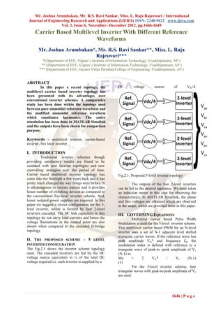
  • 1. Mr. Joshua Arumbakan, Mr. R.S. Ravi Sankar, Miss. L. Raja Rajeswari / International Journal of Engineering Research and Applications (IJERA) ISSN: 2248-9622 www.ijera.com Vol. 2, Issue 6, November- December 2012, pp.1646-1649 Carrier Based Multilevel Inverter With Different Reference Waveforms Mr. Joshua Arumbakan*, Mr. R.S. Ravi Sankar**, Miss. L. Raja Rajeswari*** *(Department of EEE, Vignan’s Institute of Information Technology, Visakhapatnam, AP.) ** (Department of EEE, Vignan’s Institute of Information Technology, Visakhapatnam, AP.) *** (Department of EEE, Gayatri Vidya Parishad College of Engineering, Visakhapatnam, AP.) ABSTRACT In this paper a recent topology, the DC voltage source of Vdc/4. multilevel carrier based inverter topology has been presented with its advantages over conventional inverter schemes. A comparative study has been done within the topology used between pure sinusoidal reference waveform and the modified sinusoidal reference waveform which constitutes harmonics. The entire simulation has been done in MATLAB Simulink and the outputs have been shown for comparison purpose. Keywords – multilevel inverter, carrier-based inverter, five level inverter I. INTRODUCTION Traditional inverter schemes though providing satisfactory results are found to be outdated with new inverter topologies and new controlling strategies over the period of time. Carrier based multilevel inverter topology has Fig.2.1. Proposed 5-level inverter topology come into the limelight a few years back and it has pretty much changed the way things were before. It The outputs of the four 2-level inverters is advantageous in various aspects and it provides can be fed to the desired appliance. We have taken lesser number of switching devices as compared to an induction motor in this case for observing the the conventional five-level inverter scheme. And, characteristics. In MATLAB Simulink, the phase lesser isolated power supplies are required. In this and line voltages are obtained which are observed paper we suggest a circuit configuration for the 5- in the scope, which are provided latter in this paper. level inverter, which is formed by four 2-level inverters cascaded. The DC link capacitors in this III. GOVERNING EQUATIONS topology do not carry load currents and hence the Multilevel carrier based Pulse Width voltage fluctuations in the neutral point are also Modulation is used for the 5-level inverter scheme. absent when compared to the cascaded H-bridge This multilevel carrier based PWM for an N-level topology. inverter uses a set of N-1 adjacent level shifted triangular carrier waves. If the reference wave has II. THE PROPOSED SCHEME – 5 LEVEL peak amplitude Vm* and frequency fm, the INVERTER CONFIGURATION modulation index is defined with reference to a The Fig.2.1 shows the inverter scheme topology triangular wave of peak-to -peak amplitude of Vc used. The cascaded inverters are fed by the DC (N-1) as voltage source equivalent to ¼ of the total DC Ma = 2 Vm* / Vc (N-1) voltage required i.e. each inverter is supplied by a (1) For the 5-level inverter scheme, four triangular waves with peak-to-peak amplitude of Vc are used. 1646 | P a g e
  • 2. Mr. Joshua Arumbakan, Mr. R.S. Ravi Sankar, Miss. L. Raja Rajeswari / International Journal of Engineering Research and Applications (IJERA) ISSN: 2248-9622 www.ijera.com Vol. 2, Issue 6, November- December 2012, pp.1646-1649 The reference waveforms used in the multilevel carrier based inverter are governed by the equations shown below: Va*=Vm Sin(ωt) + 0.2Vm Sin(3ωt) + nVc/2 (2) Vb*=Vm Sin(ωt -2π/3) + 0.2Vm Sin(3ωt) + nVc/2 (3) Vc*=Vm Sin(ωt -4π/3) + 0.2Vm Sin(3ωt) + nVc/2 (4) These reference waveforms constitute a third harmonic content which is found to improve the inverter’s performance similar to space vector modulation scheme. Control signals for the four inverters are generated such that the appropriate devices are switched to realize the particular level in a particular phase depending upon the region of operation required. The reference wave set for 2- level operation requires single triangular waveform and it increases one by one for 3-level, 4-level and 5-level as two, three and four. In this particular inverter scheme used, we are using two types of reference signals. One reference signal is a modified sinusoidal reference waveform which has harmonics in it and the other is a pure sine wave which is of null harmonics and Fig.4.2. Phase voltages-modified sine wave perfectly sinusoidal. The carrier signals and reference signals are obtained as: IV. SIMULINK BLOCKS & OUTPUTS The line voltages of the carrier based multilevel inverter topology using modified sinusoidal reference waveform is as shown below for a DC voltage of 300V. Fig.4.3. Zoomed Carrier & reference signals- Fig.4.1. Line voltages-modified sine wave modified sine wave And the phase voltages are obtained as shown below: The line voltages of the carrier based multilevel inverter topology using pure sinusoidal 1647 | P a g e
  • 3. Mr. Joshua Arumbakan, Mr. R.S. Ravi Sankar, Miss. L. Raja Rajeswari / International Journal of Engineering Research and Applications (IJERA) ISSN: 2248-9622 www.ijera.com Vol. 2, Issue 6, November- December 2012, pp.1646-1649 reference waveform is as shown below for a DC voltage of 300V. Fig.4.6. Carrier & reference signals-pure sine wave Now we compare the waveforms of the Fig.4.4. Line Voltages-pure sine wave induction motor response which is given a step And the phase voltages are obtained as shown change in torque connected to the two types of below: topologies differing in reference waveform. For modified sinusoidal reference, we obtain the Speed Vs Time plot as: Fig.4.7. Speed Vs Time-modified sine wave From the above graph it can be observed that the oscillations almost got suppressed at 0.4 sec. Now, when we consider the pure sinusoidal waveform as the reference, we can see that it’s not settling even after 0.5 sec, which is why we can give the modified sinusoidal reference signal a higher score for better performance. This can be observed if we observe the waveform in Fig.4.8. Fig.4.5. Phase Voltages-pure sine wave The carrier signals and reference signals for pure sine wave are obtained as: 1648 | P a g e
  • 4. Mr. Joshua Arumbakan, Mr. R.S. Ravi Sankar, Miss. L. Raja Rajeswari / International Journal of Engineering Research and Applications (IJERA) ISSN: 2248-9622 www.ijera.com Vol. 2, Issue 6, November- December 2012, pp.1646-1649 employing the modified sinusoidal reference waveform with harmonics in it is a better alternative compared to the purely sinusoidal reference signal; as the output waveforms observed are showing that. Also, lesser-isolated power supplies are required when compared to the cascaded H-bridge configuration & most importantly this inverter scheme also does not experience neutral-point fluctuations. The multi- level -level carrier based PWM does not require the look-up tables to realize the switching sequences as in case of space vector modulation which makes its operation and use simplified for a better Fig.4.8. Speed Vs Time-pure sine wave understanding. Now, considering the Torque Vs Time graph, for the modified sinusoidal reference waveform, we REFERENCES obtain the graph as shown below: Journal Papers:  K. Chandra Sekhar, G. Tulasi Ram Das, Multi-level inverter for Induction Motor Drive, IEEE, 2006. Nabae, I. Takahashi and H. Agaki, A new neutral point clamped PWM inverter, IEEE Transactions on Industrial Applications, volume 17, 1981,518-523.  Books:  Bimal K. Bose, Modern Power Electronics and AC Drives (Prentice Hall Fig.4.9. Torque Vs Time-modified sine wave PTR, 2002). From the above graph we can observe that the oscillations almost got minimized at 0.4 sec, and  Ned Mohan, First course in power now when we consider the case of pure sinusoidal electronics and drives (MNPERE, waveform, we observe the waveform as: Minneapolis, 2003)  Theses:  Mohammadreza Derakhshanfar, Analysis of different topologies of multilevel inverters, Master of Science Thesis, Department of Energy and Environment, Division of Electric Power Engineering, CHALMERS UNIVERSITY OF TECHNOLOGY, Göteborg, Sweden, 2010. Fig.4.10. Torque Vs Time-pure sine wave From this, we can observe that the oscillations couldn’t be suppressed even after 0.5 sec, hence proving that the modified sinusoidal reference waveform is the better alternative among the two reference signals experimented. V. CONCLUSION From the experimental results of MATLAB Simulink, we can clearly state that the multilevel carrier based inverter topology 1649 | P a g e