The microprocessor and microcontroller have similar basic components like an ALU, registers, and timing circuits. However, microcontrollers have additional built-in components like ROM, RAM, and I/O devices. Microprocessors require more external hardware and are more flexible, while microcontrollers require less external hardware but are less flexible in design. The 8051 microcontroller architecture has features like separate program and data memory, boolean processing instructions, timers/counters, serial interface, and I/O ports that can be configured in different ways.
Tamil Call Girls Bhayandar WhatsApp +91-9930687706, Best Service
8051-microcontroller
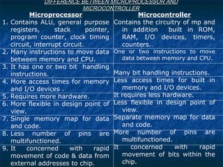
1. DIFFERENCE BETWEEN MICROPROCESSOR ANDDIFFERENCE BETWEEN MICROPROCESSOR AND
MICROCONTROLLERMICROCONTROLLER
Microprocessor
1. Contains ALU, general purpose
registers, stack pointer,
program counter, clock timing
circuit, interrupt circuit.
2. Many instructions to move data
between memory and CPU.
3. It has one or two bit handling
instructions.
4. More access times for memory
and I/O devices .
5. Requires more hardware.
6. More flexible in design point of
view.
7. Single memory map for data
and code.
8. Less number of pins are
multifunctioned.
9. It concerned with rapid
movement of code & data from
external addresses to chip.
Microcontroller
Contains the circuitry of mp and
in addition built in ROM,
RAM, I/O devices, timers,
counters.
One or two instructions to move
data between memory and CPU.
Many bit handling instructions.
Less access times for built in
memory and I/O devices.
It requires less hardware.
Less flexible in design point of
view.
Separate memory map for data
and code.
More number of pins are
multifunctioned.
It concerned with rapid
movement of bits within the
chip.
3. Microcontroller Survey
Microcontroller RAM ROM Counters I/O pins Other features
4-bit 256 4K 2 14 ADC, WDT
(M34501) (4-bit) (10 bit)
8-bit 128 4K 2 32 UART
(8051) bytes
16-bit 4K 8K 2 24 Counter array, ADC,
(68HC16Z3) bytes WDT
32-bit 32K 4 64 Color LCD Controller
bytes 3 UART,WDT,DMA,
PLL, Real time clock
4. Difference between RISC and CISC Processor
RISC CISC
1. Simple instructions taking one cycle Complex instructions taking multiple
cycles
2. Very few instructions refer memory Most instructions may refer memory
3. Instructions are executed by hardware Instructions are executed by
microprogram.
4. Few instructions Many instructions
5. Fixed format instructions Variable format instructions
6. Few addressing modes Many addressing modes
7. Multiple register set Single register set
8. Highly pipelined Not pipelined or less pipelined
9. Conditional jump can be based on Conditional jump is usually based on
a bit anywhere in memory. Status register bit.
5. TCY0 TCY1 TCY2 TCY3
Fetch1 Execute 1
Fetch2 Execute 2
Fetch3 Execute 3
Pipelining or parallelism
means fetching for next
instruction while executing
current instruction.
CPU
Memory
CP
U
Data Memory Program Memory
Von-Neumann or Princeton Harvard
6.
7. Von-nuemann Architecture Harvard Architecture
1. Programs and data share the same Uses separate memory for programs and
memory space. Data.
2. Program and data fetches are done No need to have TDM for address and data
using TDM which affect performance. buses.
3. Code storage may not be optimal & Optimal code storage. Allows instn to be
requires multiple fetches to form prefetched & decoded while multiple data
instrn. being fetched & operated on.
Eg. Motorola 68HC11 mc PIC mc, MCS-51
8. 8051 Architecture
Features:
1. Operating frequency is 12MHz
2. Separate 64K program and data memory
3. Multiply and divide instructions are available.
4. Boolean processor (operates on single bit)
5. 32 I/O lines can be used as four 8-bit ports (P0-P3) or 32 I/O
lines.
6. Two 16-bit Timers/Counters.
7. Serial interface : Full duplex serial data receiver/transmitter.
8. 4K bytes ROM
9. 128 bytes RAM
10.Two external interrupts through INTO and INT1 pins
30. If you use a frequency source
as a crystal oscillator,
If you use a frequency source
as a TTL oscillator,
Oscillator
31. I/O PORTSI/O PORTS
Total 4 ports
1. Port 0 may serve as inputs, outputs, or as a low order
address and data bus for external memory.
2. Port 1 may be used as input/output port.
3. Port 2 may be used as input/output or high order
address byte.
4. Port 3 may be used as an input/output and for some
alternate function.
Each port consists of a latch, an output driver, and an
input buffer.
32. The bit latch is represented as a TypeD flipflop, which will clock in a value from
the internal bus in response to a “write to latch” signal, Q output of the flipflop is
placed on the internal bus in response to a “read latch” signal, level of the port
pin itself is placed on the internal bus in response to a “read pin” signal from the
CPU.
The output drivers of PortsO and2 are switchable to an internal ADDR and
ADDR/DATA bus by an internal CONTROL signal for use in external memory
access.
If P3 bit latch contains a 1, then the output level is controlled by the signal
“alternate output function". The actual P3.X pin level is always available to the
pin’s “alternate input function”.
To be used as an input, the port bit latch must contain a 1, which turns off the
output driver FET. Then, for Ports 1, 2, and 3, the pin is pulled high by the
internal pullup, but can be pulled low by an external source.
Because Ports 1, 2, and 3 have fixed internal pullups they are sometimes
called “qussi-bidirectional”ports as inputs they pull high and will source current
when externally pulled low. Port O, is “true” bidirectional, because when
configured as an input it floats.
To be used as an output, the port bit latch must contain a 0,which turns on the
output driver FET.