SlideShare una empresa de Scribd logo
1 de 30
Descargar para leer sin conexión
1
Electron Microscopy II
Transmission - , Scanning Transmission - and
Analytical Electron Microscopy
krumeich@inorg.chem.ethz.ch
www.microscopy.ethz.ch
Electron Microscopy Methods
Transmission Electron Microscopy (TEM)
Bright / Dark Field (BF/DF)
High-Resolution Transition Electron Microscopy (HRTEM)
Energy-Filtered (EFTEM)
Electron Diffraction (ED)
Scanning Transmission Electron Microscopy (STEM)
Bright / Dark Field (BF/DF-STEM)
High-Angle Annular Dark Field (HAADF-STEM)
Analytical Electron Microscopy (AEM)
X-ray Spectroscopy
Electron Energy-Loss Spectroscopy (EELS)
Electron Spectroscopic Imaging (ESI)
Scanning Electron Microscopy (SEM)
Secondary Electrons (SE)
Back-Scattered Electrons (BSE)
2
Development of the First Transmission
Electron Microscope
Knoll, Ruska, Z. Phys. 78 (1932) 318
1927 Hans Busch: Electron beams
can be focused in an inhomogeneous
magnetic field.
1931 Max Knoll and Ernst Ruska
built the first TEM.
1986 Nobel prize for Ruska
History of Electron Microscopy
1938 First Siemens electron microscope (resolution ca. 13 nm)
History of Electron Microscopy
3
1939: first TEM serially
produced by Siemens
resolution ca. 7 nm
History of Electron Microscopy
Transmission Electron Microscopes
∼1970: HRTEM
Philips EM400, V = 120 kV
resolution ca. 0.35 nm
∼1990
Philips CM30, V = 300 kV
resolution ca. 0.2 nm
Transmission Electron Microscopy
Magnetic Lens
An electron in a magnetic
field (here: inhomogeneous,
but axially symmetric)
experiences the Lorentz
force F:
F = -e (E + v x B)
|F| = evBsin(v,B)
E: strength of electric field
B: strength of magnetic field
e/v: charge/velocity of electrons
4
Transmission Electron Microscopy
Magnetic Lens
Lens
Back focal plane
Image plane
Object plane
Light optical analogue
Lens equation: 1/u + 1/v = 1/f
Magnification M = v/u
Lens problems:
spherical aberation Cs
chromatic aberation Cc
astigmatism
Transmission Electron Microscopy
Cross-Section of the Column of a CM30 Microscope
accelerator
electron gun
condenser system
objective lenses
sample
diffraction lens
intermediate lens
projector lenses
viewing screen
photo camera
TV, SlowScan
CCD Camera
5
Electron Guns
Thermoionic Guns
Electron emission by heating
Transmission Electron Microscopy
Field Emission Guns
(FEG)
Electron emission by applying
an extraction voltage
W
W
LaB6
>1000500100Lifetime / h
10135x1010109Brightness / A/m2sr
(30-)3005001000Maximum current / nA
3-20500030000Source size / nm
0.4-1.51.5-33-4Energy spread / eV
(300-)180020002700Temperature / K
4.52.44.5Work function / eV
FEGLaB6WProperties
TEM – Imaging and Diffraction
Optic axis
Objective lens
Back focal plane
Image plane
Object plane
↓
Diffraction pattern
Transmission Electron Microscopy
6
TEM – Imaging and Diffraction
Optic axis
Image plane
Diffraction pattern
Transmission Electron Microscopy
Diffraction and Imaging Mode
Transmission Electron Microscopy
7
TEM – Imaging and Diffraction
Optic axis
Diffraction pattern
Image
Bright field image
- mass-thickness contrast
- Bragg contrast
Transmission Electron Microscopy
TEM – Imaging and Diffraction
Optic axis
Diffraction pattern
Image Dark field image
Transmission Electron Microscopy
8
Elastic Scattering of Electrons by an Atom
Transmission Electron Microscopy
Weak Coulomb interaction within the
electron cloud
⇒ low-angle scattering
Strong Coulomb interaction with the
nucleus
⇒ scattering into high angles or even
backwards (Rutherford scattering)
⇒ atomic-number (Z) contrast
Types of Image Contrast
Mass-Thickness contrast
Transmission Electron Microscopy
Bragg contrast
Coherent scattering
Diffracted beams do not pass through the
objective aperture leading to a decreased
intensity of crystalline areas
9
BF Images
Transmission Electron Microscopy
Amorphous SiO2 on C foil
Mainly thickness contrast
Au particles (black) on TiO2
Mainly mass contrast
Increasing thickness
BF Images
Transmission Electron Microscopy
ZrO2 micro crystals; crystals orientated close
to zone axis appear dark
Mainly Bragg contrast
Increasing thickness
10
BF and DF imaging
Pt-Particles in SiO2 nanotubes
Transmission Electron Microscopy
BF DF conical DF
TEM – Imaging and Diffraction
Optic axis
Image plane
Diffraction pattern
Transmission Electron Microscopy
11
TEM – Imaging and Diffraction
Optic axis
Diffraction pattern
Image
High-resolution image
Interference of several
diffracted beams with the
direct beam
Transmission Electron Microscopy
TEM – Imaging and Diffraction
Optic axis
Diffraction pattern
Image
Mathematics
+
-2i qx
-
{f(x)} ( ) e dx
∞
π
∞
= ∫F f x
Fourier Transform
Fourier analysis
Fourier synthesis
Transmission Electron Microscopy
12
TEM – Imaging and Diffraction
Optic axis
Diffraction pattern
HRTEM image
Image Processing
Fourier Transform
Fourier Transform
Filtered image
Transmission Electron Microscopy
ED + HRTEM
Nb8W9O47 – threefold TTB
superstructure
Transmission Electron Microscopy
13
HRTEM: Detection of Defects
Planar defect in ZnNb14O35F2
Transmission Electron Microscopy
HRTEM: Detection of Defects
Grain boundary between differently
ordered areas in a Nb-W oxide
Transmission Electron Microscopy
10 nm
14
HRTEM and ED of Aperiodic Structures
Dodecagonal quasicrystal in the system Ta-Te
Transmission Electron Microscopy
HRTEM: Imaging Single Atoms
Gd@C82 in SWCNT
Suenaga et al, Science 290 (2000) 2280
3 nm
3 nm
Transmission Electron Microscopy
15
Transmission Electron Microscopy
Contrast:
• Mass-thickness (BF/DF)
• Bragg (BF/DF)
• Phase (HRTEM)
Determination of
• Structure: HRTEM
• Defects: HRTEM, TEM
• Lattice constants and symmetry: ED
• Particle size: TEM, HRTEM
Transmission Electron Microscopy
Scanning Transmission Electron
Microscopy (STEM)
Scanning Transmission Electron Microscopy
From: Williams, Carter: Transmission Electron Microscopy
16
BF and DF Imaging in STEM
Au islands
on a C film
DF image
recorded by the
annular dark
field detector
BF image
recorded by the
bright field
detector
Scanning Transmission Electron Microscopy
From: Williams, Carter: Transmission Electron Microscopy
STEM
Detectors
BF: Bright Field detector
ADF: Annular Dark Field detector
HAADF: High Angle Annular Dark Field detector
Scanning Transmission Electron Microscopy
10 mrad ≈ 0.57°
From: Williams, Carter: Transmission Electron Microscopy
17
BF and DF Imaging in STEM
Scanning Transmission Electron Microscopy
Pt Particles in SiO2 nanotubes
BF ADF HAADF
BF DF conical DF TEM
HAADF-STEM or Z contrast Images of
Au Particles on Titania
Scanning Transmission Electron Microscopy
50 nm
10 nm
18
High-Resolution HAADF-STEM
WO3 segregations in a
bronze-type Nb-W oxide
Scanning Transmission Electron Microscopy
HRTEM
2 nm
HAADF-STEM of Nb8W9O47
Information about Elemental Distribution
in HAADF-STEM or Z contrast images
Single-crystal X-ray structure
of Nb8W9O47
ca. 80% Nb 100% W
P21212 a=12.26, b=36.63, c=3.95 Å
ca. 80% Nb100% W
19
Scanning Transmission Electron
Microscopy
Contrast:
• Mass-thickness (BF/DF)
• Bragg (BF/DF)
• Z2 (HAADF)
Determination of
• Particles on support: HAADF
• Structure and defects : HR
Important: Combination with EDXS or EELS
Scanning Transmission Electron Microscopy
Interactions of Electrons with Matter
XEDS (EDX, EDS),
WDS, EPMA
SEM
SEM
AES
elastic scattering:
TEM, HRTEM,
STEM, SAED, CBED
inelastic scattering:
EELS, ESI
specimen
electron
beam
scattered
electrons
direct
beam
X rays
backscattered
electrons
Auger
electrons
secondary
electrons
20
Generation of X-rays
1. Ionization
2. X-ray emission
Analytical Transmission Electron Microscopy
Generation of X-rays
1. Ionization
2. X-ray
emission
Inelastic interactions
α1 α2
β1
α1
21
Electron Configuration of Ti: 1s2 2s2 2p6 3s2 3p6 4s2 3d2
energy
1s
2s
3s
4s
2p
3p
4p
3d
K
L
M
N
Kα
Kβ
Inelastic interactions
Energy-Dispersive X-ray Spectroscopy (EDXS)
Analytical Transmission Electron Microscopy
Au-Particles on TiO2
Intensity/counts
Energy / keV
Deceleration of incident
electrons by interaction
with Coulomb field of
nucleus leads to
uncharacteristic
spectrum background
(bremsstrahlung).
Ti L
22
Possible Transitions Between Electron Shells
causing characteristic K, L, M X-rays
Analytical Transmission Electron Microscopy
Quantitative EDXS
Cliff-Lorimer Equation:
NA/NB = kAB IA/IB
NA,NB: atomic % of element A,B
IA/IB: measured intensity of element A,B
kAB: Cliff-Lorimer factor
Analytical Transmission Electron Microscopy
23
X-ray Spectrometer
Analytical Transmission Electron Microscopy
Schematic representation of a energy-dispersive spectrometer with
electronic units. Spectrometers can be attached to TEMs and SEMs.
STEM @ EDXS: Point Analyses
HAADF-STEM of Pd/Pt
particles on alumina
Analytical Transmission Electron Microscopy
Pt
Pd
Pt
Pt
Cu
Al
O
C
Pt
Pd
Pt Pt
Cu
Al
O
C
24
STEM @ EDXS: Point Analyses
500 nm
1
HAADF Detector
Energy (keV)
Counts
20151050
60
40
20
0
W
W
W WW
W
Mo
MoM
Mo
Mo MoMo
Cu
Cu
EDX HAADF Detector Point 1
Analytical Transmission Electron Microscopy
(Mo,W)Ox or
MoOx and WOx?
Interactions of Electrons with Matter
XEDS (EDX, EDS),
WDS, EPMA
SEM
SEM
AES
elastic scattering:
TEM, HRTEM,
STEM, SAED, CBED
inelastic scattering:
EELS, ESI
specimen
electron
beam
scattered
electrons
direct
beam
X rays
backscattered
electrons
Auger
electrons
secondary
electrons
Phonons: lattice vibrations (sample
heating)
Plasmons: electron gas oscillations
Cathodoluminescence: electron-
holes in semiconductors
25
Electron Energy Loss Spectroscopy (EELS)
Analytical Transmission Electron Microscopy
Electron Energy Loss Spectroscopy
Analytical Transmission Electron Microscopy
Relationship between the EEL Spectrum and a Core-Loss
Exication within the Band Structure
ELNES:
Electron Energy Loss Near
Edge Structure
reflects local density of
unoccupied states corresponds
to XANES
EXELFS:
EXtended Energy Loss Fine
Structure
information on local atomic
arrangements corresponds to
EXAFS
Filled states Empty states
EF E
N(E)
Extended fine
structure
Near edge
fine structure
26
Fine structures in EELS
Analytical Transmission Electron Microscopy
Characteristics of the C_K edge
depending on hybridization
Characteristics of the Cu_L2,3
edges depending on oxidation
state of Cu
HRTEM and EELS: Imaging and Detection of
Single Atoms
Gd@C82 in SWCNT
Suenaga et al, Science 290 (2000) 2280
3 nm
3 nm
Transmission Electron Microscopy
27
Elemental Maps by Electron
Spectroscopic Imaging (ESI)
Post-column filter
gun
round lens
sample holder
aperture (objective and sel. area)
aperture (filter entrance)
prism (with straight edges)
prism (with curved edges)
energy-selecting slit
quadrupole lens
sextupole lens
CCD camera
Energy-filtered image
EELS (section) of VOx-NTs
3 window method
Analytical Transmission Electron Microscopy
Elemental Maps by Electron
Spectroscopic Imaging (ESI)
TEM image Vanadium map Carbon map
V and C, respectively, are located at the
sites appearing with bright contrast.
Analytical Transmission Electron Microscopy
28
Imaging of Elemental Distribution
TEM image Ag_M map
M edge: 367 eV
Au_M map
M edge: 2206 eV
Ag/Au Particles on Silica
Analytical Transmission Electron Microscopy
EELS (EFTEM) versus EDXS (x-ray mapping)
Slow technique; only simple
processing required
Fast technique; but complex
processing required
Inefficient signal generation, collection
and detection
=> inefficient x-ray mapping
Very efficient and higher sensitivity to
most elements
=> very efficient mapping technique
Energy resolution > 100 eV causes
frequent overlaps
Energy resolution 0.3-2 eV results in
far fewer overlaps; fine structures
X-rays provide elemental information
only
Elemental, chemical and dielectric
information
High detection efficiency for high Z
elements
High detection efficiency for low Z
elements
EDXSEELS
Analytical Transmission Electron Microscopy
29
Analytical Electron Microscopy
• Qualitative and quantitative information about
the composition: EDXS, EELS
• Bonding, coordination, interatomic distances:
Fine structure in EELS (ELNES, EXEFS)
• Locally resolved information about composition
1. STEM + EDXS and/or EELS
2. ESI
Analytical Transmission Electron Microscopy
Analytical Electron Microscopy
- Restrictions
• Electron-matter interactions are mostly elastic
⇒ high electron dose necessary
• Long recording times
⇒ high sample stability and absence of drift
• Ionization edges occur at different energies and
are of different shape
⇒ not all methods are equally suitable for
all elements
Analytical Transmission Electron Microscopy
30
Analytical Electron Microscopy
- Restrictions
signal/noise measuring time
spatial resolution
Analytical Transmission Electron Microscopy

Más contenido relacionado

La actualidad más candente

Raman spectroscopy of carbon-nanotubes
Raman spectroscopy of carbon-nanotubesRaman spectroscopy of carbon-nanotubes
Raman spectroscopy of carbon-nanotubesajay singh
 
Applications of metal nanoparticles in photocatalysis
Applications of metal nanoparticles in photocatalysisApplications of metal nanoparticles in photocatalysis
Applications of metal nanoparticles in photocatalysisChamudithaBenaragama
 
carbon dots and its applications
carbon dots and its applicationscarbon dots and its applications
carbon dots and its applicationspchandrasekaran
 
XRF Theory and Application
XRF Theory and ApplicationXRF Theory and Application
XRF Theory and ApplicationSirwan Hasan
 
Dye sensitized solar cells
Dye sensitized solar cellsDye sensitized solar cells
Dye sensitized solar cellsAshish Singh
 
Ellipsometry- non destructive measuring method
Ellipsometry- non destructive measuring methodEllipsometry- non destructive measuring method
Ellipsometry- non destructive measuring methodViji Vijitha
 
Quantum dots and their applications
Quantum dots and their applicationsQuantum dots and their applications
Quantum dots and their applicationsDragon5588
 
Analysis of SAED patterns
Analysis of SAED patternsAnalysis of SAED patterns
Analysis of SAED patternsAntilen Jacob
 
Hydrothermal synthesis and characterization of one
Hydrothermal synthesis and characterization of oneHydrothermal synthesis and characterization of one
Hydrothermal synthesis and characterization of oneAlexander Decker
 
Scanning electron microscopy
Scanning electron microscopyScanning electron microscopy
Scanning electron microscopyGanesh Shinde
 
Mossbauer Spectroscopy
Mossbauer SpectroscopyMossbauer Spectroscopy
Mossbauer SpectroscopyMANISHSAHU106
 
Application of Carbon dots ppt
Application of Carbon dots pptApplication of Carbon dots ppt
Application of Carbon dots pptAxy Patil
 
Quantum dots 1
Quantum dots 1Quantum dots 1
Quantum dots 1Ashraf Ali
 
x ray crystallography & diffraction
x ray crystallography & diffractionx ray crystallography & diffraction
x ray crystallography & diffractionArman Dalal
 
Doping the quantum dots
Doping the quantum dotsDoping the quantum dots
Doping the quantum dotsAhmad Aly
 
DYE SENSITIZED SOLAR CELLS
DYE SENSITIZED SOLAR CELLSDYE SENSITIZED SOLAR CELLS
DYE SENSITIZED SOLAR CELLSThiru Ram
 

La actualidad más candente (20)

Raman spectroscopy of carbon-nanotubes
Raman spectroscopy of carbon-nanotubesRaman spectroscopy of carbon-nanotubes
Raman spectroscopy of carbon-nanotubes
 
Applications of metal nanoparticles in photocatalysis
Applications of metal nanoparticles in photocatalysisApplications of metal nanoparticles in photocatalysis
Applications of metal nanoparticles in photocatalysis
 
carbon dots and its applications
carbon dots and its applicationscarbon dots and its applications
carbon dots and its applications
 
XRF Theory and Application
XRF Theory and ApplicationXRF Theory and Application
XRF Theory and Application
 
Dye sensitized solar cells
Dye sensitized solar cellsDye sensitized solar cells
Dye sensitized solar cells
 
Ellipsometry- non destructive measuring method
Ellipsometry- non destructive measuring methodEllipsometry- non destructive measuring method
Ellipsometry- non destructive measuring method
 
Quantum dots and their applications
Quantum dots and their applicationsQuantum dots and their applications
Quantum dots and their applications
 
Analysis of SAED patterns
Analysis of SAED patternsAnalysis of SAED patterns
Analysis of SAED patterns
 
Hydrothermal synthesis and characterization of one
Hydrothermal synthesis and characterization of oneHydrothermal synthesis and characterization of one
Hydrothermal synthesis and characterization of one
 
Scanning electron microscopy
Scanning electron microscopyScanning electron microscopy
Scanning electron microscopy
 
xrd basic
 xrd basic xrd basic
xrd basic
 
Mossbauer Spectroscopy
Mossbauer SpectroscopyMossbauer Spectroscopy
Mossbauer Spectroscopy
 
Anusha
AnushaAnusha
Anusha
 
Application of Carbon dots ppt
Application of Carbon dots pptApplication of Carbon dots ppt
Application of Carbon dots ppt
 
Quantum dots 1
Quantum dots 1Quantum dots 1
Quantum dots 1
 
x ray crystallography & diffraction
x ray crystallography & diffractionx ray crystallography & diffraction
x ray crystallography & diffraction
 
Tem ppt
Tem pptTem ppt
Tem ppt
 
Doping the quantum dots
Doping the quantum dotsDoping the quantum dots
Doping the quantum dots
 
Xrd presentation [autosaved] [autosaved] copy (2)
Xrd presentation [autosaved] [autosaved]   copy (2)Xrd presentation [autosaved] [autosaved]   copy (2)
Xrd presentation [autosaved] [autosaved] copy (2)
 
DYE SENSITIZED SOLAR CELLS
DYE SENSITIZED SOLAR CELLSDYE SENSITIZED SOLAR CELLS
DYE SENSITIZED SOLAR CELLS
 

Similar a Electron microscopy 2

Microprobing with electrons
Microprobing with electronsMicroprobing with electrons
Microprobing with electronsJonathan Price
 
Atomic Plane Resolution Electron Magnetic Circular Dichroism
Atomic Plane Resolution Electron Magnetic Circular DichroismAtomic Plane Resolution Electron Magnetic Circular Dichroism
Atomic Plane Resolution Electron Magnetic Circular DichroismRiccardo Di Stefano
 
Scanning electron microscopy
Scanning electron microscopy Scanning electron microscopy
Scanning electron microscopy SimmiiiChoudhary
 
SCANNING ELECTRON MICROSCOPE MITHILESH CHOUDHARY
SCANNING ELECTRON MICROSCOPE MITHILESH CHOUDHARYSCANNING ELECTRON MICROSCOPE MITHILESH CHOUDHARY
SCANNING ELECTRON MICROSCOPE MITHILESH CHOUDHARYAnjan Anant
 
2018 ELECTRON DIFFRACTION AND APPLICATIONS
2018 ELECTRON DIFFRACTION AND APPLICATIONS2018 ELECTRON DIFFRACTION AND APPLICATIONS
2018 ELECTRON DIFFRACTION AND APPLICATIONSHarsh Mohan
 
X ray Photoelectron Spectroscopy (XPS)
X ray Photoelectron Spectroscopy (XPS)X ray Photoelectron Spectroscopy (XPS)
X ray Photoelectron Spectroscopy (XPS)Nano Encryption
 
X ray Photoelectron spectroscopy (XPS)
X ray Photoelectron spectroscopy (XPS)X ray Photoelectron spectroscopy (XPS)
X ray Photoelectron spectroscopy (XPS)Nano Encryption
 
X ray photoelectron spectroscopy (xps)
X ray photoelectron spectroscopy (xps)X ray photoelectron spectroscopy (xps)
X ray photoelectron spectroscopy (xps)Nano Encryption
 
Transmission Electron Microscope
Transmission Electron MicroscopeTransmission Electron Microscope
Transmission Electron MicroscopeManoranjan Ghosh
 
Materials Characterization
Materials CharacterizationMaterials Characterization
Materials CharacterizationVikas Barnwal
 

Similar a Electron microscopy 2 (20)

Scanning Electron Microscope
Scanning Electron MicroscopeScanning Electron Microscope
Scanning Electron Microscope
 
SEM BRIEF.docx
SEM BRIEF.docxSEM BRIEF.docx
SEM BRIEF.docx
 
Sem Poster
Sem PosterSem Poster
Sem Poster
 
Microprobing with electrons
Microprobing with electronsMicroprobing with electrons
Microprobing with electrons
 
SEM-for MS.pptx
SEM-for MS.pptxSEM-for MS.pptx
SEM-for MS.pptx
 
Tem
TemTem
Tem
 
Atomic Plane Resolution Electron Magnetic Circular Dichroism
Atomic Plane Resolution Electron Magnetic Circular DichroismAtomic Plane Resolution Electron Magnetic Circular Dichroism
Atomic Plane Resolution Electron Magnetic Circular Dichroism
 
Xps
XpsXps
Xps
 
Analysis of diffraction patterns generated through TEM
Analysis of diffraction patterns generated through TEMAnalysis of diffraction patterns generated through TEM
Analysis of diffraction patterns generated through TEM
 
SEM.ppt
SEM.pptSEM.ppt
SEM.ppt
 
Scanning electron microscopy
Scanning electron microscopy Scanning electron microscopy
Scanning electron microscopy
 
SCANNING ELECTRON MICROSCOPE MITHILESH CHOUDHARY
SCANNING ELECTRON MICROSCOPE MITHILESH CHOUDHARYSCANNING ELECTRON MICROSCOPE MITHILESH CHOUDHARY
SCANNING ELECTRON MICROSCOPE MITHILESH CHOUDHARY
 
2018 ELECTRON DIFFRACTION AND APPLICATIONS
2018 ELECTRON DIFFRACTION AND APPLICATIONS2018 ELECTRON DIFFRACTION AND APPLICATIONS
2018 ELECTRON DIFFRACTION AND APPLICATIONS
 
6. Nanomaterials
6. Nanomaterials6. Nanomaterials
6. Nanomaterials
 
X ray Photoelectron Spectroscopy (XPS)
X ray Photoelectron Spectroscopy (XPS)X ray Photoelectron Spectroscopy (XPS)
X ray Photoelectron Spectroscopy (XPS)
 
X ray Photoelectron spectroscopy (XPS)
X ray Photoelectron spectroscopy (XPS)X ray Photoelectron spectroscopy (XPS)
X ray Photoelectron spectroscopy (XPS)
 
X ray photoelectron spectroscopy (xps)
X ray photoelectron spectroscopy (xps)X ray photoelectron spectroscopy (xps)
X ray photoelectron spectroscopy (xps)
 
Transmission Electron Microscope
Transmission Electron MicroscopeTransmission Electron Microscope
Transmission Electron Microscope
 
Materials Characterization
Materials CharacterizationMaterials Characterization
Materials Characterization
 
Electron Microscopy
Electron MicroscopyElectron Microscopy
Electron Microscopy
 

Más de José da Silva Rabelo Neto

Aplicação do método de rietveld para análise quantitativa de fases dos polimo...
Aplicação do método de rietveld para análise quantitativa de fases dos polimo...Aplicação do método de rietveld para análise quantitativa de fases dos polimo...
Aplicação do método de rietveld para análise quantitativa de fases dos polimo...José da Silva Rabelo Neto
 
The "state of the art" of diffraction analysis of crystallite size and lattic...
The "state of the art" of diffraction analysis of crystallite size and lattic...The "state of the art" of diffraction analysis of crystallite size and lattic...
The "state of the art" of diffraction analysis of crystallite size and lattic...José da Silva Rabelo Neto
 
Introduction Quantitative X-Ray Diffraction Methods
Introduction Quantitative X-Ray Diffraction MethodsIntroduction Quantitative X-Ray Diffraction Methods
Introduction Quantitative X-Ray Diffraction MethodsJosé da Silva Rabelo Neto
 
Feynman physics lectures v1 ch30 1962 02-23 diffraction
Feynman physics lectures v1 ch30 1962 02-23 diffractionFeynman physics lectures v1 ch30 1962 02-23 diffraction
Feynman physics lectures v1 ch30 1962 02-23 diffractionJosé da Silva Rabelo Neto
 

Más de José da Silva Rabelo Neto (20)

Jeol2000 fx inst
Jeol2000 fx instJeol2000 fx inst
Jeol2000 fx inst
 
Jeol 2010 basic_easyusing
Jeol 2010 basic_easyusingJeol 2010 basic_easyusing
Jeol 2010 basic_easyusing
 
Transmission electron microscopy 1
Transmission electron microscopy 1Transmission electron microscopy 1
Transmission electron microscopy 1
 
Transmission electron microscopy 2
Transmission electron microscopy 2Transmission electron microscopy 2
Transmission electron microscopy 2
 
Atomic force microscopy
Atomic force microscopyAtomic force microscopy
Atomic force microscopy
 
Stm afm
Stm afmStm afm
Stm afm
 
Gsas intro rvd (1)
Gsas intro rvd (1)Gsas intro rvd (1)
Gsas intro rvd (1)
 
Tutorial gsas
Tutorial gsasTutorial gsas
Tutorial gsas
 
Dissert girao2 difracao
Dissert girao2 difracaoDissert girao2 difracao
Dissert girao2 difracao
 
Difracao de raios X wfa
Difracao de raios X wfaDifracao de raios X wfa
Difracao de raios X wfa
 
Difracao de raios X
Difracao de raios XDifracao de raios X
Difracao de raios X
 
Crystal sizeanalysis
Crystal sizeanalysisCrystal sizeanalysis
Crystal sizeanalysis
 
Aplicação do método de rietveld para análise quantitativa de fases dos polimo...
Aplicação do método de rietveld para análise quantitativa de fases dos polimo...Aplicação do método de rietveld para análise quantitativa de fases dos polimo...
Aplicação do método de rietveld para análise quantitativa de fases dos polimo...
 
The "state of the art" of diffraction analysis of crystallite size and lattic...
The "state of the art" of diffraction analysis of crystallite size and lattic...The "state of the art" of diffraction analysis of crystallite size and lattic...
The "state of the art" of diffraction analysis of crystallite size and lattic...
 
Crystallite size nanomaterials
Crystallite size   nanomaterialsCrystallite size   nanomaterials
Crystallite size nanomaterials
 
Introduction Quantitative X-Ray Diffraction Methods
Introduction Quantitative X-Ray Diffraction MethodsIntroduction Quantitative X-Ray Diffraction Methods
Introduction Quantitative X-Ray Diffraction Methods
 
10 xrd-software
10 xrd-software10 xrd-software
10 xrd-software
 
X ray diffraction basics
X ray diffraction basicsX ray diffraction basics
X ray diffraction basics
 
Feynman physics lectures v1 ch30 1962 02-23 diffraction
Feynman physics lectures v1 ch30 1962 02-23 diffractionFeynman physics lectures v1 ch30 1962 02-23 diffraction
Feynman physics lectures v1 ch30 1962 02-23 diffraction
 
10 xrd-software
10 xrd-software10 xrd-software
10 xrd-software
 

Electron microscopy 2

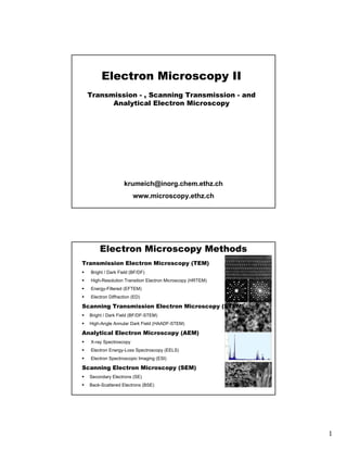
  • 1. 1 Electron Microscopy II Transmission - , Scanning Transmission - and Analytical Electron Microscopy krumeich@inorg.chem.ethz.ch www.microscopy.ethz.ch Electron Microscopy Methods Transmission Electron Microscopy (TEM) Bright / Dark Field (BF/DF) High-Resolution Transition Electron Microscopy (HRTEM) Energy-Filtered (EFTEM) Electron Diffraction (ED) Scanning Transmission Electron Microscopy (STEM) Bright / Dark Field (BF/DF-STEM) High-Angle Annular Dark Field (HAADF-STEM) Analytical Electron Microscopy (AEM) X-ray Spectroscopy Electron Energy-Loss Spectroscopy (EELS) Electron Spectroscopic Imaging (ESI) Scanning Electron Microscopy (SEM) Secondary Electrons (SE) Back-Scattered Electrons (BSE)
  • 2. 2 Development of the First Transmission Electron Microscope Knoll, Ruska, Z. Phys. 78 (1932) 318 1927 Hans Busch: Electron beams can be focused in an inhomogeneous magnetic field. 1931 Max Knoll and Ernst Ruska built the first TEM. 1986 Nobel prize for Ruska History of Electron Microscopy 1938 First Siemens electron microscope (resolution ca. 13 nm) History of Electron Microscopy
  • 3. 3 1939: first TEM serially produced by Siemens resolution ca. 7 nm History of Electron Microscopy Transmission Electron Microscopes ∼1970: HRTEM Philips EM400, V = 120 kV resolution ca. 0.35 nm ∼1990 Philips CM30, V = 300 kV resolution ca. 0.2 nm Transmission Electron Microscopy Magnetic Lens An electron in a magnetic field (here: inhomogeneous, but axially symmetric) experiences the Lorentz force F: F = -e (E + v x B) |F| = evBsin(v,B) E: strength of electric field B: strength of magnetic field e/v: charge/velocity of electrons
  • 4. 4 Transmission Electron Microscopy Magnetic Lens Lens Back focal plane Image plane Object plane Light optical analogue Lens equation: 1/u + 1/v = 1/f Magnification M = v/u Lens problems: spherical aberation Cs chromatic aberation Cc astigmatism Transmission Electron Microscopy Cross-Section of the Column of a CM30 Microscope accelerator electron gun condenser system objective lenses sample diffraction lens intermediate lens projector lenses viewing screen photo camera TV, SlowScan CCD Camera
  • 5. 5 Electron Guns Thermoionic Guns Electron emission by heating Transmission Electron Microscopy Field Emission Guns (FEG) Electron emission by applying an extraction voltage W W LaB6 >1000500100Lifetime / h 10135x1010109Brightness / A/m2sr (30-)3005001000Maximum current / nA 3-20500030000Source size / nm 0.4-1.51.5-33-4Energy spread / eV (300-)180020002700Temperature / K 4.52.44.5Work function / eV FEGLaB6WProperties TEM – Imaging and Diffraction Optic axis Objective lens Back focal plane Image plane Object plane ↓ Diffraction pattern Transmission Electron Microscopy
  • 6. 6 TEM – Imaging and Diffraction Optic axis Image plane Diffraction pattern Transmission Electron Microscopy Diffraction and Imaging Mode Transmission Electron Microscopy
  • 7. 7 TEM – Imaging and Diffraction Optic axis Diffraction pattern Image Bright field image - mass-thickness contrast - Bragg contrast Transmission Electron Microscopy TEM – Imaging and Diffraction Optic axis Diffraction pattern Image Dark field image Transmission Electron Microscopy
  • 8. 8 Elastic Scattering of Electrons by an Atom Transmission Electron Microscopy Weak Coulomb interaction within the electron cloud ⇒ low-angle scattering Strong Coulomb interaction with the nucleus ⇒ scattering into high angles or even backwards (Rutherford scattering) ⇒ atomic-number (Z) contrast Types of Image Contrast Mass-Thickness contrast Transmission Electron Microscopy Bragg contrast Coherent scattering Diffracted beams do not pass through the objective aperture leading to a decreased intensity of crystalline areas
  • 9. 9 BF Images Transmission Electron Microscopy Amorphous SiO2 on C foil Mainly thickness contrast Au particles (black) on TiO2 Mainly mass contrast Increasing thickness BF Images Transmission Electron Microscopy ZrO2 micro crystals; crystals orientated close to zone axis appear dark Mainly Bragg contrast Increasing thickness
  • 10. 10 BF and DF imaging Pt-Particles in SiO2 nanotubes Transmission Electron Microscopy BF DF conical DF TEM – Imaging and Diffraction Optic axis Image plane Diffraction pattern Transmission Electron Microscopy
  • 11. 11 TEM – Imaging and Diffraction Optic axis Diffraction pattern Image High-resolution image Interference of several diffracted beams with the direct beam Transmission Electron Microscopy TEM – Imaging and Diffraction Optic axis Diffraction pattern Image Mathematics + -2i qx - {f(x)} ( ) e dx ∞ π ∞ = ∫F f x Fourier Transform Fourier analysis Fourier synthesis Transmission Electron Microscopy
  • 12. 12 TEM – Imaging and Diffraction Optic axis Diffraction pattern HRTEM image Image Processing Fourier Transform Fourier Transform Filtered image Transmission Electron Microscopy ED + HRTEM Nb8W9O47 – threefold TTB superstructure Transmission Electron Microscopy
  • 13. 13 HRTEM: Detection of Defects Planar defect in ZnNb14O35F2 Transmission Electron Microscopy HRTEM: Detection of Defects Grain boundary between differently ordered areas in a Nb-W oxide Transmission Electron Microscopy 10 nm
  • 14. 14 HRTEM and ED of Aperiodic Structures Dodecagonal quasicrystal in the system Ta-Te Transmission Electron Microscopy HRTEM: Imaging Single Atoms Gd@C82 in SWCNT Suenaga et al, Science 290 (2000) 2280 3 nm 3 nm Transmission Electron Microscopy
  • 15. 15 Transmission Electron Microscopy Contrast: • Mass-thickness (BF/DF) • Bragg (BF/DF) • Phase (HRTEM) Determination of • Structure: HRTEM • Defects: HRTEM, TEM • Lattice constants and symmetry: ED • Particle size: TEM, HRTEM Transmission Electron Microscopy Scanning Transmission Electron Microscopy (STEM) Scanning Transmission Electron Microscopy From: Williams, Carter: Transmission Electron Microscopy
  • 16. 16 BF and DF Imaging in STEM Au islands on a C film DF image recorded by the annular dark field detector BF image recorded by the bright field detector Scanning Transmission Electron Microscopy From: Williams, Carter: Transmission Electron Microscopy STEM Detectors BF: Bright Field detector ADF: Annular Dark Field detector HAADF: High Angle Annular Dark Field detector Scanning Transmission Electron Microscopy 10 mrad ≈ 0.57° From: Williams, Carter: Transmission Electron Microscopy
  • 17. 17 BF and DF Imaging in STEM Scanning Transmission Electron Microscopy Pt Particles in SiO2 nanotubes BF ADF HAADF BF DF conical DF TEM HAADF-STEM or Z contrast Images of Au Particles on Titania Scanning Transmission Electron Microscopy 50 nm 10 nm
  • 18. 18 High-Resolution HAADF-STEM WO3 segregations in a bronze-type Nb-W oxide Scanning Transmission Electron Microscopy HRTEM 2 nm HAADF-STEM of Nb8W9O47 Information about Elemental Distribution in HAADF-STEM or Z contrast images Single-crystal X-ray structure of Nb8W9O47 ca. 80% Nb 100% W P21212 a=12.26, b=36.63, c=3.95 Å ca. 80% Nb100% W
  • 19. 19 Scanning Transmission Electron Microscopy Contrast: • Mass-thickness (BF/DF) • Bragg (BF/DF) • Z2 (HAADF) Determination of • Particles on support: HAADF • Structure and defects : HR Important: Combination with EDXS or EELS Scanning Transmission Electron Microscopy Interactions of Electrons with Matter XEDS (EDX, EDS), WDS, EPMA SEM SEM AES elastic scattering: TEM, HRTEM, STEM, SAED, CBED inelastic scattering: EELS, ESI specimen electron beam scattered electrons direct beam X rays backscattered electrons Auger electrons secondary electrons
  • 20. 20 Generation of X-rays 1. Ionization 2. X-ray emission Analytical Transmission Electron Microscopy Generation of X-rays 1. Ionization 2. X-ray emission Inelastic interactions α1 α2 β1 α1
  • 21. 21 Electron Configuration of Ti: 1s2 2s2 2p6 3s2 3p6 4s2 3d2 energy 1s 2s 3s 4s 2p 3p 4p 3d K L M N Kα Kβ Inelastic interactions Energy-Dispersive X-ray Spectroscopy (EDXS) Analytical Transmission Electron Microscopy Au-Particles on TiO2 Intensity/counts Energy / keV Deceleration of incident electrons by interaction with Coulomb field of nucleus leads to uncharacteristic spectrum background (bremsstrahlung). Ti L
  • 22. 22 Possible Transitions Between Electron Shells causing characteristic K, L, M X-rays Analytical Transmission Electron Microscopy Quantitative EDXS Cliff-Lorimer Equation: NA/NB = kAB IA/IB NA,NB: atomic % of element A,B IA/IB: measured intensity of element A,B kAB: Cliff-Lorimer factor Analytical Transmission Electron Microscopy
  • 23. 23 X-ray Spectrometer Analytical Transmission Electron Microscopy Schematic representation of a energy-dispersive spectrometer with electronic units. Spectrometers can be attached to TEMs and SEMs. STEM @ EDXS: Point Analyses HAADF-STEM of Pd/Pt particles on alumina Analytical Transmission Electron Microscopy Pt Pd Pt Pt Cu Al O C Pt Pd Pt Pt Cu Al O C
  • 24. 24 STEM @ EDXS: Point Analyses 500 nm 1 HAADF Detector Energy (keV) Counts 20151050 60 40 20 0 W W W WW W Mo MoM Mo Mo MoMo Cu Cu EDX HAADF Detector Point 1 Analytical Transmission Electron Microscopy (Mo,W)Ox or MoOx and WOx? Interactions of Electrons with Matter XEDS (EDX, EDS), WDS, EPMA SEM SEM AES elastic scattering: TEM, HRTEM, STEM, SAED, CBED inelastic scattering: EELS, ESI specimen electron beam scattered electrons direct beam X rays backscattered electrons Auger electrons secondary electrons Phonons: lattice vibrations (sample heating) Plasmons: electron gas oscillations Cathodoluminescence: electron- holes in semiconductors
  • 25. 25 Electron Energy Loss Spectroscopy (EELS) Analytical Transmission Electron Microscopy Electron Energy Loss Spectroscopy Analytical Transmission Electron Microscopy Relationship between the EEL Spectrum and a Core-Loss Exication within the Band Structure ELNES: Electron Energy Loss Near Edge Structure reflects local density of unoccupied states corresponds to XANES EXELFS: EXtended Energy Loss Fine Structure information on local atomic arrangements corresponds to EXAFS Filled states Empty states EF E N(E) Extended fine structure Near edge fine structure
  • 26. 26 Fine structures in EELS Analytical Transmission Electron Microscopy Characteristics of the C_K edge depending on hybridization Characteristics of the Cu_L2,3 edges depending on oxidation state of Cu HRTEM and EELS: Imaging and Detection of Single Atoms Gd@C82 in SWCNT Suenaga et al, Science 290 (2000) 2280 3 nm 3 nm Transmission Electron Microscopy
  • 27. 27 Elemental Maps by Electron Spectroscopic Imaging (ESI) Post-column filter gun round lens sample holder aperture (objective and sel. area) aperture (filter entrance) prism (with straight edges) prism (with curved edges) energy-selecting slit quadrupole lens sextupole lens CCD camera Energy-filtered image EELS (section) of VOx-NTs 3 window method Analytical Transmission Electron Microscopy Elemental Maps by Electron Spectroscopic Imaging (ESI) TEM image Vanadium map Carbon map V and C, respectively, are located at the sites appearing with bright contrast. Analytical Transmission Electron Microscopy
  • 28. 28 Imaging of Elemental Distribution TEM image Ag_M map M edge: 367 eV Au_M map M edge: 2206 eV Ag/Au Particles on Silica Analytical Transmission Electron Microscopy EELS (EFTEM) versus EDXS (x-ray mapping) Slow technique; only simple processing required Fast technique; but complex processing required Inefficient signal generation, collection and detection => inefficient x-ray mapping Very efficient and higher sensitivity to most elements => very efficient mapping technique Energy resolution > 100 eV causes frequent overlaps Energy resolution 0.3-2 eV results in far fewer overlaps; fine structures X-rays provide elemental information only Elemental, chemical and dielectric information High detection efficiency for high Z elements High detection efficiency for low Z elements EDXSEELS Analytical Transmission Electron Microscopy
  • 29. 29 Analytical Electron Microscopy • Qualitative and quantitative information about the composition: EDXS, EELS • Bonding, coordination, interatomic distances: Fine structure in EELS (ELNES, EXEFS) • Locally resolved information about composition 1. STEM + EDXS and/or EELS 2. ESI Analytical Transmission Electron Microscopy Analytical Electron Microscopy - Restrictions • Electron-matter interactions are mostly elastic ⇒ high electron dose necessary • Long recording times ⇒ high sample stability and absence of drift • Ionization edges occur at different energies and are of different shape ⇒ not all methods are equally suitable for all elements Analytical Transmission Electron Microscopy
  • 30. 30 Analytical Electron Microscopy - Restrictions signal/noise measuring time spatial resolution Analytical Transmission Electron Microscopy