SlideShare una empresa de Scribd logo
1 de 23
Descargar para leer sin conexión
SOLIDS
1
Types of Solid
Amorphous Solid
Atoms are irregularly placed so these solids do not have characteristic shapes. e.g. Glass, rubber,
plastic, quartz glass.
(1) They do not have sharp m.pt.
(2) They are isotropic (show similar optical & electrical properties like refractive index,
thermal expansion etc. in all direction).
(3) These are super cooled liquid or pseudo solids because like liquids,
amorphous solids have tendency to flow though very slowly. Glass panes
fixed to windows or doors of old buildings are invariably found to be
slightly thicker at the bottom than at the top. This is because the glass flow
down very slowly and makes the bottom portion slightly thicker. Some glass
objects from ancient civilizations are found to become milky in appearance
because of some crystalisation.
(4) They do not have well defined planes
(5) They do not have symmetry.
Crystalline Solid (all solid elements and compounds, quartz)
Atoms are regularly or orderly arranged.
(1) Have sharp m. pt (2) Anisotropic (3) Crystal are bound by plane
faces
(4) They have plane of symmetry, centre of symmetry (always one) and axis of symmetry.
Isotropy and Anisotropy
Amorphous substance are said to be isotropic because they exhibit the same optical & electrical
property in all directions. In amorphous solids; refractive index, thermal and electrical
conductivities, coefficient of thermal expansion, are independent of the direction along which
they are measured.
Crystalline substances, on the other hand, are anisotropic and the magnitude of a physical
property varies with directions. This arises due to different arrangement of particles in different
directions. For example, in a crystal of silver iodide, the coefficient of thermal expansion is
positive in one direction and negative in other.
Explanation of Isotropy and Anisotropy
In amorphous substance, as in liquids, the arrangement of
particles is random and disordered. Therefore, all directions are
equivalent and properties are independent of direction. On the
other hand, the particles in a crystal are arranged and well
ordered. Thus, the arrangement of particles may be different
directions.
Distinction between Crystalline and Amorphous Solids
Property Crystalline Solids Amorphous Solids
Shape Definite characteristic
geometrical shape
Irregular shape
Melting point Melt at a sharp and characteristic
temperature
Gradually soften over a range of
temperature
Cleavage property When cut with a sharp edged tool,
they split into two pieces and the
newly generated surfaces are
plain and smooth
When cut with a sharp edged tool,
they cut into two pieces with
irregular surfaces
Heat of fusion They have a definite and They do not have a definite and
SOLIDS
2
characteristic heat of fusion characteristic heat of fusion.
Anisotropy Anisotropic in nature. Mechanical
strength, electrical & properties
changes with direction
Isotropic in nature. Mechanical
strength, electrical & optical
properties are same in all
direction.
Nature True solids Pseudo solids or super cooled
liquids
Order in arrangement
of constituent
particles
Long range order Only short range order
Long range and short range : If in a solid, arrangement of particles follows regular and
periodic pattern for short distance only it is called short range order and if regular and periodic
pattern is observed in whole crystal its called long range order.
Classification of Crystalline Solid:
Type of
Solid
Constituent
Particles
Nature of Forces Examples Characteristics Properties
1. Ionic Positive
and
negative
ions
Strong electrostatic
forces of attraction
NaCl, KNO3, LiF,
MgO
Hard, brittle, high melting
points (~ 1500 K), soluble in
polar solvents, insulator in the
solid state, good conductor in
the molten state or aqueous
solution.
2.
Molecular
Molecules 1.Non polar
molecular solid-
vander Waal’s
forces
2.Hydrogen bond
mol solid
3. Polar mol solid-
dipole dipole
interaction
l2, Cl2, solid CO2
(dry ice), and Ar,
CH4, Napthalene,
glucose sulphur,
ice
Solid SO2, solid
NH3
Soft, low melting points, low
density, volatile and insulators
of heat and electricity.
3. Network
or
Covalent
Atoms Covalent bonds C (Diamond and
graphite), Si, SiO2,
SiC Boron, Black
Very hard with very high
melting point (~ 4000 K) and
insulators (except graphite)
4. Metallic Atoms Metallic bond i.e.
Attraction between
positive metal ions
(kernels) and
mobile electrons
All metals and
some alloys
Range from soft to very hard,
high melting points
(~ 800 – 1000 K) malleable and
ductile, possess lustre, good
conductors of heat and
electricity.
Explanation for the Metallic Properties
The different physical properties of the metals mentioned earlier can be explained with the help
of electron sea model for the metallic bonds. These are disused as follows:
1. Electrical Conductivity
According to electron sea model, the electrons present in the sea are mobile but their
movement is not systematic. When a potential difference is applied by placing electrodes
on both sides of a metal, the movement of the electrons becomes systematic. They flow
from cathode to the anode. As a result, the electrical current flows across a metal or it
becomes conducting.
The electrical conductivity of metals decreases with the rise in temperature. Actually
when temperature increases, the average kinetic energy of the positively charged kernels
SOLIDS
3
also increases. They start moving in the electron sea and obstruct the movement of the
electrons leading decreased electrical conductivity.
2. Thermal conductivity
When we heat a certain portion of a metal the kinetic energy of the electrons present
increases. They move towards the colder regions and collide with the electrons with less
kinetic energy. As a result, kinetic energy is transferred. Thus, heat is conducted through
the metal .
3. Malleability and ductility
We know that the metals are malleable (can be beaten into sheets) and ductile (can be
drawn into wires). Both these characteristics can be explained with the help of electron
sea model. When stress is applied on the metal surface, the kernels present in a particular
layer slip over the other layer. The crystal lattice or the shape of the crystal gets
deformed as a result of it. However, the environment of the kernels remains the same i.e.
mobile electrons keep on attracting the kernels. Only there is a shift in the position of the
kernels from the one lattice site to the other.
4. Metallic Lustre
Metals have generally a shining surface known as lustre. This lustre is also due to the
mobile electrons. When light falls on the surface of a metal, the electrons absorb photons
and start vibrating at a frequency equal to that of the incident light. These vibrating
electrons emit electromagnetic radiations in the form of light. As a result, the metal
surface acquires a shining appearance known as lustre.
5. High tensile strength
This is the property of the metal as a result of which they can be stretched without
breaking. The tensile strength is because of strong electrostatic force of attraction
between the kernels and mobile electrons.
6. Hardness of metals
The hardness of metals is related to the strength of the the metallic bonds between the
kernels and the mobile electrons. Greater the number of these electrons, stronger will be
the bond. Similarly, smaller the size of the kernels, greater will be their attraction for the
electrons. For example, sodium is very soft because the size oif the kernel is large and
there is only one valence electron.
Q. Why solids are hard and rigid?
A. Solids are hard and rigid because the intermolecular distances between solids are very
less and the intermolecular forces operating between the molecules are very strong. Thus
the molecules in solids are packed very close to each other. Hence they cannot move about
freely and can only vibrate about their positions.
Q. Why solids have definite volume?
A. Any matter that is a solid has a definite shape and a definite volume. The molecules in
a solid are in fixed positions and are close together. Although the molecules can still vibrate,
they cannot move from one part of the solid to another part. As a result, a solid does not
easily change its shape or its volume.
Q. Ionic solids are hard and rigid in nature?
A. In ionic crystal the lattice is made of positive and negative ions. These are held together by
ionic bonds – the strong electrostatic attractions between oppositely charged ions.
Consequently, the cations and anions attract one another and pack together in an arrangement
so that the attractive forces maximize. Each ion is surrounded by neighbours of opposite charge
and there are no separate molecules. Since the ions are fixed in their lattice sites, typical ionic
solids are hard and rigid with high melting points.
Q. Ionic solids are brittle?
SOLIDS
4
A. On hammering or applying stress a layer of ions slips away from their oppositely charged
neighbours and brings them closer to ions of like charge. The increase of electrostatic repulsions
along the displaced plane causes the crystal to break.
Space Lattice and Unit Cell
Space Lattice:
The geometrical form consisting only of a regular array of points (atoms, molecules, ion)
in space is called space lattice or it can be defined as an array of points showing how
molecules, atoms or ions are arranged in different sites in three dimensional space. The
sites which are occupied by constituent units (molecules ions or atoms) are called lattice
points.
Unit Cell:
It is defined as the smallest building block of a solid which
when repeated over and again results into the space
lattice. We must specify the unit cell by length of its edges
and the angles between them.
Parameters of a unit cell:
A unit cell is characterized by :
(i) Its dimensions (lengths) along the three edges as ‘a’, ‘b’ and ‘c’. These edges may or may
not be mutually perpendicular.
(ii) Angles ,  and  between the pair of edges. The angle  is between the edges b and c,
angle  is between the edges c and a and angle  is between the edges a and b. Thus, a unit
cell is characterized by six parameters, a, b, c, ,  and .
IMPORTANT unit cell:
Cubic cell a = b = c  =  =  = 90o
Monoclinic a  b  c  =  = 90o   90o
Hexagonal a = b  c  =  = 90o,
Triclinic a  b  c       90o
Note : Cubic is the most stable and symmetrical while triclinic least stable and unsymmetrical.
Types of unit cell:
i) Primitive or simple unit cell
When a unit cell contain constituent particles only at corners ,it is called primitive unit
cell
ii) Non –Primitive unit cells
When a unit cell contain one or more constituent particles at corners & some other
positions. It is called centered unit cell. There are three types non–primitive unit cell e.g.
i) Body centred : – When lattice points are at corners & centre of unit cell.
SOLIDS
5
ii) Face centred: – When lattice points are at corners & centre of each face of unit cell
iii) End centred: – When lattice points are at corners & centre of two opposite faces.
Effective Number of Atoms Per Unit Cell (Rank of Unit Cell)
1. Atom at the corner of unit cell is shared by 8 unit cells. Thus, contribution of each corner
atom (per unit cell) is 1/8.
2. Atom present at the face of a unit cell is shared by 2 unit cells. Contribution of face atom
(per unit cell) is 1/2.
3. For atom present at the centre of unit cell, contribution per unit cell is equal to 1.
4. For atom present at the edge of unit cell is shared by 4 unit cells. Contribution of edge
atom (per unit cell) is 1/4.
(1) Rank for Cubic Unit Cell
It is the effective number of atoms present in cell. It is represented by Z.
nc = no. of corner atoms,
nf = no. of face atoms
nb = no. of body atoms (inside the cube)
ne = no. of edge atoms
Rank = b
efC
n
4
n
2
n
8
n
 for cubic unit cell
Assignment – I
Q.1 A compound formed by elements X and Y crystallizes in the cubic structure where Y
atoms are at the corners of the cube and X atoms are at the alternate faces. What is the
formula of the compound?
Q.2 If three elements P, Q and R crystallize in a cubic solid lattice with P atoms at the
corners, Q atoms at the cube centre and R atoms at the centre of the faces of the cube,
then write the formula of the compound.
Q.3 Potassium crystallizes in a body–centred cubic lattice. Calculate the approximate
number of unit cells in 2g potassium. Atomic mass of potassium  39u.
Q.4 In a face centred lattice of X and Y, X atoms are present at the corners while Y atoms are
at face centres. Then the formula of the compound if one of the X atoms is missing from a
corner in each unit cell would be:
(a) X7Y24 (b) X24Y7 (c) XY24 (d) X24Y
SOLIDS
6
Packing of Spheres in Solids:
(A) Close Packing in One Dimension
Close packing of spheres in one dimension.
(B) Close Packing in Two Dimensions
(b) Three dimensional close packing from two dimensional hexagonal close packed
layers
In the first layer there are some empty spaces or hollows called voids. These are
triangular in shape. These triangular voids are of two types marked as a and b. All the
hollows are equivalent but the spheres of second layer may be placed either on hollows
which are marked a or on other set of hollows marked b. It may be noted that it is not
possible to place spheres on both types of hollows. Let us place the spheres on hollows
market b to make the second layer which may be labeled as B layer. Obviously the holes
marked ‘a’ remain unoccupied while building the second layer.
Whenever a sphere of second layer is placed above the void of first layer, a tetrahedral
void is formed. These voids are called tetrahedral voids because a tetrahedral is formed
when the centres of these four spheres are joined. There are marked at ‘T’ voids.
The voids ‘a’ are double triangular voids. The triangle void in the second layer are above
the triangular voids in the first layer and the triangular shapes of these voids do not
overlap. One of them has the apex of the triangle pointing upward & other downward.
Such voids are surrounded by six spheres and are called octahedral voids.
Now the third layer can be build up by placing spheres above tetrahedral voids or
octahedral voids.
SOLIDS
7
(II) Placing Third Layer over the Second Layer:
When third layer is placed over the second, there are two possibilities.
(a) Covering tetrahedral voids
When a third layer is to be added, again there are two types of void available. One type of
void marked ‘a’ are unoccupied hollows of the first layer. The other type of void are void
in the second layer (marked c). Thus, there are two alternative to build the third layer.
Tetrahhedral Void
Octahedral Void
SOLIDS
8
Solid Circle Represent Layer A and Dotted Actual view of hexagonal close
packing
Circle Represent Layer B
The third layer of sphere may be placed on the tetrahedral voids marked (c) of the
second layer. In this arrangement, the spheres of the third layer lie directly above those
in the first layer. In other words, third layer becomes exactly identical to the first layer
(labelled A).
As shown in figure.
Simplified view of Hexagonal close packing (AB AB …… pattern)
This type of packing is referred to as ABABA …. arrangement. This type of packing is also
known as hexagonal close packing. This type of arrangement is found in many metals
like Mg and Zn.
(b) Covering octahedral voids
The second way to pack spheres in the third layer is to place them over octahedral voids
marked ‘a’ (unoccupied void of first layer). This gives rise to a new layer labeled as C.
Sphere of third layer are not alligned with first layer or second layer. However, it can be
shown that the spheres in the fourth layer will correspond to those in the first layer.
As shown in figure.
SOLIDS
9
This type packing is called as the ABCABCA ….. type of arrangement. It is also known as
cubic close packing( ccp) or face centred cubic arrangement (fcc).
It may be noted that both types of packing are equally economical though these have
different forms. In both cases, 74% of the available volume is occupies by the spheres and
co–ordination no equal to12 . Metals like Cu & Ag crystallies in FCC pattern.
(c) Body centred cubic close packing (ABAB …. Type) Co–ordination No. = 8
In this packing atom of each layer will not touch any other atom of the same layer but
four atoms of one layer will touch to same atom of second layer. In this packing unit cell
will be BCC and arrangement of first and third layer will be same
Important facts about Unit cells and the Packing of Spheres in Crystalline Solids
(i). Particles pack together in crystals so that they can be as close together as possible
to maximize intermolecular attractions.
(ii). Simple cubic packing – the spheres in one layer sit directly on top of those in the
previous layer.
(AAA……)
1. All layers are identical having both vertical and horizontal alignment of
atoms.
2. Primitive – cubic unit cell.
3. Coordination number = 6. Sphere touches four neighbours in the same
layer, one above and one below.
4. Uses only 52% of available volume.
(iii). Body – centered cubic packing – spheres are in alternate layers in an ABAB…..
arrangements where the spheres in the B layers fit into the small depressions
between spheres in the neighbouring layers. Atoms of each layer will not touch to
each other but four atoms of same layer will touch to same atom of 2nd layer.
1. Body – centered cubic cell.
SOLIDS
10
2. Coordination number = 8; four neighbours above and four neighbours
below
3. Occupies 68% of the available volume.
4. S–Block elements forms BCC unit cell
(iv). Hexagonal close packing– noncubic unit cell with two alternating layer (ABAB……)
1. Hexagonal arrangement of touching spheres.
2. Spheres in B layer fit into the small triangular depressions between
spheres of A layer.
3. Coordination number = 12
4. Six neighbours in the same layer, three above and three below.
(v). Cubic close packing– face centered cubic unit cell with three alternating layers,
(ABCABC …...)
1. A – B layers identical to hexagonal close packing
2. Third layer is offset from both A and B.
3. Co–ordination number 12
4. Transition metal forms FCC unit cell
(vi) Cubic is the most symmetrical while triclinic is the most unsymmetrical system.
(vii).
Sr.
No.
Structure Type of
packing
Stacking pattern Coordinatio
n number
Space
used
(%)
Unit cell
(a) Simple
cubic
Square
close
packing
AAA … 6 52 Primitive cubic
(b) Body
centred
cubic
Square
close
packing
ABAB….. 8 68 Body centred
cubic
(c) Hexagonal
close
packed
Hexagonal ABAB… 12 74 (Non–cubic)
(d) Cubic
close
packed
Hexagonal ABCABC… 12 74 Face centred
cubic
(viii) In FCC or CCP there are three different layers which are constantly repeated in
three dimensions. In HCP every first & third layers are same and in ccp every first
& fourth layers are same.
Between A & B (in close packing) the Octahedral & tetrahedral voids are located.
If we place atoms of 3rd layer over the tetrahedral void, the layer A will be
repeated, hence ABAB….. structure or HCP will be formed.
If we place atoms of third layer over Octahedral void, then FCC will be generated as
third layer will be different layer & it is ABCABC ….. type.
The number of nearest neighbours for any atom, molecule or ion in a space lattice
is called the coordination number.
Type of Cubic Unit Cell & Packing Fraction
1. Simple or Primitive Cubic Unit Cell:
SOLIDS
11
2. Body–Centred Cubic Unit Cell (BCC Unit Cell)
3. Face centred Cubic Unit Cell (FCC Unit Cell)
Radius Ratio for the octahedral void under ideal condition.
SOLIDS
12
Radius Ratio of Tetrahedral Void
Body diagonal of smaller cube & larger cube are collinear & body diagonal of smaller cube is
exactly half the larger cube. Body diagonal of smaller cube =
2
1
× Body diagonal of larger cube
cubeerarglofdiagonalBody
4
1
rr ac 
a3
4
1
rr ac  ….. (1)
In FCC unit cell 4ra = a2 …… (2)
from (1) & (2)
aac r
2
3
rr 
1
2
3
r
r
a
c

= 0.225
Thus, for an atom to occupy a tetrahedral void, its radius must be 0.225 times the radius of the
sphere
Radius Ratio Rules
For the stability of an compound, each cation should be surrounded by maximum number of
anions and vice versa (for maximum electrostatic forces of attraction). The number of
oppositely charged ions surroundings each ions is called its co–ordination number.
Since ionic bond is non–directional, the arrangement of ions within the ionic crystal is
determined by the sizes of the ions.
The ratio of the radius of the cation to that of the anion is called radius ratio, i.e.
atomhostofRadius
atomquestofRadius
)r(aniontheofRadius
)r(cationtheofRadius
RatioRadius
a
c

The guest atom must make a contact with host atom but host atom may or may not make
contact. Evidently, greater is the radius ratio, the larger is the size of the cation and hence
greater is its co–ordination number. The relationships between the radius ratio and the co–
ordination number and the structural arrangement are called radius ratio rules, and are given in
Table.
Radius ratio rules for AB type structures
Radius Ratio Co–
ordination no
Structural
arrangement
Structure type Examples
=0.155 but <
0.225
3 Planar triangular – B2O3
=0.225 but <0.414 4 Tetrahedral Sphalerite, ZnS CuCl, CuBr, Cul, BaS
=0.414 but <
0.732
6 Octahedral Sodium
chloride (Rock
salt)
HgS, NaBr, KBr,
MgO, MnO, CaO, CaS
=0.732 but <1.0 8 Body–centred
cubic
Caseium
chloride
Csl, CsBr, TlBr,
NH4Br
The increase in coordination number with increase in radius ratio can be easily understood by
considering a particular cation (so that its size i.e. r+ remains constant) and arranging anions of
decreasing size around it (so that r– decreases and hence r+/r– increases). We observe that as
the radius ratio increases, the number of anions touching the cation increases i.e. coordination
number increases
SOLIDS
13
Illustrating effect of radius ratio on co–ordination number. As rc/ra increases, coordination
number increases
Q. 1 Atoms of element B from hcp lattice and those of the element A occupy 2/3rd of tetrahedral
voids. What is the formula of the compound formed by these elements A and B?
Q.2 In a crystalline solid, anions B are arranged in a cubic close packing. Cations A are equally
distributed between octahedral and tetrahedral voids. If all the octahedral voids are
occupied, what is the formula of the solid?
Q.3 In the mineral, spinel, having the formula MgAl2O4, oxide ions are arranged in the cubic close
packing, Mg2+ ions occupy the tetrahedral voids while Al3+ ions occupy the octahedral
voids.
(i) What percentage of tetrahedral voids is occupied by Mg2+ ions?
(ii) What percentage of octahedral voids is occupied by Al3+ ions?
Q.4 In a solid oxide ions are arranged in cubic close packing. One-sixth of the tetrahedral
voids are occupied by cations A while one-third of the octahedral void are occupied by
the cations B. What is the formula of the solid?
Q.5 B– ions form a close packed structure. If the radius of B– ion is 195 pm, calculate the
radius of the cation that just fits into the tetrahedral hole. Can a cation A+ having a radius
of 82 pm be slipped into the octahedral hole of the crystal A+ B–?
Q.6 If the close packed cations in an NaCl type solid have a radius of 75 pm, what would be
the maximum and minimum sizes of the anions forming the voids?
Density of Cubic Unit Cell
In NaCl type unit cell, d = rc + ra = a/2
In CsCl type d = rc + ra = a
2
3
[2d = Body diagonal]
In ZnS type 4ra = a2
Q.1 CsCl has cubic structure. Its density is 4.0g cm–3. What is the distance between Cs+ and
Cl– ions? (At. mass of Cs = 133) 357 pm
SOLIDS
14
Solid defect
Electronic
imperfecton
Atomic imperfection
(Point defect)
Stoichiometric defect
If number of cation & anion
remain same after the defect so
stoichiometry will be preserved
Non stoichiometric defect
No. of cation & anion ratio
changes so stoichiometry is
distrubed by this defect
Impurity defect
Schottky
defect
Frenkel
defect
Due to deficiency
of metal
Due to excess
of metal
Interstitial if impurity
atoms are small
Substitutional if
impurity atoms are
of same size as
that of host atoms
Due to presence of extra metal ions Due to anion vacancies (F - centre)
Q.2 An element has a body–centred cubic (bcc) structure with edge of 288 pm. The density
of the element is 7.2g/cm3. How many atoms are present in 208g of the element?
24.17 × 10²³ atoms
Q.3 KF has NaCl structure. If the distance between K+ and F– is 269 pm, find the density of
KF(NA = 6.02  1023 mol–1, atomic masses K = 39, F = 19 amu). 2.48 gm/cm3
Q.4 Calculate the density of silver which crystallizes in a face–centred cubic structure. The
distance between the nearest silver atoms in this structure is 287 pm. (Molar mass of Ag
=107.87g mol –1, NA = 6.02  1023 mol–1) 10.71 gm/cm3
Q.5 The density of a face centred cubic element (atomic mass = 60.2 amu) is 6.25g cm–3.
Calculate the length of the edge of the unit cell. 4 × 10⁻⁸ cm
Q.6 What is the distance between Na+ and Cl– in a NaCl crystal if its density is 2.165g cm–3?
NaCl crystallizes in the fcc lattice. 281 pm
Defect in Solid
Ionic crystals can have perfect arrangement only at absolute zero temperature. According to
third law of thermodynamics, S = 0 only at 0 K. At any temperature above 0 K, the crystals have
some departure from complete ordered arrangement. With increase of temperature S will
increase so G will becomes more negative (G = H – TS). Even single crystals which are
grown with all care and which appear to be perfect may contain some internal irregularities. So
the process of defect formation will become more prominent. Hence solid defect is a natural
phenomenon. Any deviation from completely ordered arrangement in a crystal constitutes a
disorder or a defect. The crystal may have defects due to the presence of some impurities.
1. Electronic Imperfection
These correspond to defects due to the electrons. In perfect crystal at 0 K electrons are
present the fully occupied lowest energy states. But at higher temperature (above 0 K),
some of the electrons may occupy higher energy states, depending upon the temperature.
These electrons become free to move and therefore, they are responsible for the
electrical conductivity. The atom from which electrons have been removed become
electron deficient and these are referred to as holes. The holes also give rise to electrical
conductivity, but the direction of motion of holes in an electric field is opposite to that of
SOLIDS
15
the electrons. Free electrons and holes in crystals are considered to be electronic
imperfections. These electronic imperfections are responsible for electrical
conductance.
2. Point Defect
If atoms are missing from lattice point, displaced or extra ions are present, it is called
point defects [electrical neutrality of the crystal is never affected by any kind of defect].
There are three types of point defects
(a) Stoichiometric defect (b) Non–stoichiometric (c) Impurity defects
(A) Stoichiometric defect:
In which stoichiometry of crystal is maintained even after the defect. i.e. Number of
positive & negative ions are exactly in the same ratios as in non–defected solids.
(i) Schottky defect
It is basically a vacancy defect in ionic solid. When a crystal site become vacant by
removal of a structural unit in the lattice, then the defect is referred to as the vacancy
defect. In an ionic crystal, a cation and anion may leave the lattice to cause two vacancies.
Such a defect which involves equal no of cation and anion vacancies in the crystal lattice
is called a schottky defect. Cation vacancy is followed by anion vacancy leading to
decrease in density.
Compound with high Co. no. & high ionic character shows this defect. The crystal
begins to conduct electricity to a smaller extent by ionic mechanism. The stability of the
crystal is lowered. e.g. NaCl, CsCl. It has been observed that in NaCl, there are about 106
Schottky pair per cm3. In 1 cm3 there are about 1022 ions. Thus there is one schottky
defect per 1016 ion.
(ii) Frenkel Defect
This defect is shown by ionic solids. The small ion (usually cation) is dislocated from its
normal site to an interstitial site. It creates a vacancy defect at its original site & an
interstitial defect at its new location. Small ions are displaced from their standard lattice
point and present in non–standard lattice points i.e. interstitial. This is also called
dislocation defect. It does not change the density of the solid as atoms are not absent
from lattice they are just displaced. This defect is shown by those ionic solids in which
there is a large difference in size of ions and low co.od(less ionic character] e.g. Zng,
AgCl, Agl, AgBr due to presence of small Zn+2 and Ag+ .
AgBr shows both Schottky and Frenkel defect. (It is because AgBr crystal has a
coordination number of 6 which is neither high nor low. The radius ratio of AgBr is also
intermediate, thus AgBr satisfies the conditions to exhibit both type of defects.)
Consequences of Schottky and Frenkel Defect
Schottky & Frenkel defects in crystals lead to some interesting consequences. These are given
below:
1. Because of the presence of these defects, the electrical conductivity of crystal increases.
When an electric field is applied, a nearby ion moves from its lattice site to occupy a
‘hole’. This results in creating a new ‘hole’ and another nearby ion moves into it and so
on. This process continues and hole, thereby, move from one end to the another end.
Thus, it conducts electricity across the whole of the crystal.
SOLIDS
16
2. Due to the presence of holes in the crystal, its density decreases. However it may be
noted that density decreases only for crystals having Schottky defects.
3. The presence of ‘holes’ also decreases the lattice energy or the stability of the crystal. The
presence of too many holes may cause a partial collapse of the lattice.
B. Point Defects in Non–Stoichiometric Crystals
The compounds in which the ratio of positive and negative ions present in the compound
differs from that required by ideal chemical formula of the compound are called non–
stoichiometric compounds. The defects in these compounds are called non–
stoichiometric defects.
These are of two types depending upon whether positive ions are in excess or negative
ions are in excess. These are also known as metal excess defects and metal deficiency
defects respectively.
(A) Metal Excess Defects
In these defects, the positive ions are in excess. These may arise due to the following two
ways:
(i) Anion vacancies
In this case, negative ions may be missing from their lattice sites leaving holes in which
the electrons remain entrapped to maintain the electrical neutrality. Evidently, there is
an excess of positive (metal) ions although the crystal as a whole is electrically neutral.
This type of defect is observed in those crystals which are likely to form Schottky defects.
For example, in alkali metal halide, anion vacancies are produced when alkali metal
halide crystals are heated in the atmosphere of the alkali metal vapours. The metal atoms
get deposited on the surface of the alkali metal halide crystal, halide ions move into the
surface and combine with metal atoms.
The electrons, thus produced by the ionization of the metal atoms diffuse into the crystal
and get trapped at the anion vacancies. The electrons trapped in anion vacancies are
referred to as F–centre (from German word farbe centre for colour centre). These give
very interesting colours. For example
(i)LiCl crystal appear pink when heated in presence of Li vapours..
(ii)NaCl crystal appear yellow when heated in presence of Na vapours.
(iii)KCl crystal appear pink when heated in presence of K vapours.
(ii) Excess cations occupying interstitial sites
In this case, there are extra positive ions occupying interstitial sites and the electrons in
another interstitial sites to maintain electrical neutrality. This type of defect is found in
crystals which are likely to develop Frenkel defect. The common example is zinc oxide.
Zinc oxide (ZnO) loses oxygen reversibly at high temperatures and turns yellow in colour.
The excess Zn2+ ions are trapped in interstitial sites and equal number of electrons are
trapped in the neighbourhood to balance the electrical charge. There is excess of zinc in
the crystal and its formula becomes Zn(1 + x) O. These free electrons are responsible for
conductance. This is the only defect where density increases.
2
2
O
2
1
e2ZnZnO  
Electron remains trapped in
Anion vacancy (F – centre)
SOLIDS
17
Consequences of Metal Excess Defects
1. The crystal with metal excess defects conducts electricity due to the presence of the
electrons. These compounds are also called n–type semi–conductors since the current
is carried by the electrons in the normal way.
2. The crystals with metal excess defects are generally coloured. For example, non–
stoichiometric sodium chloride is yellow, non–stoichiometric potassium chloride is
violet.
(B) Metal Deficiency Defects
There are many solids which are difficult to prepare in stoichiometric composition and
contain less amount of the metal as compared to the stoichiometric proportion. Mostly
this happens with transition metal salts. e.g. FeO which is mostly found with a
composition of Fe0.95O. It may actually range from Fe0.93O to Fe0.95O. In crystals of FeO
some Fe+2 cations are missing and the loss of positive charge is made up by the presence
of required number of Fe+3 ion. Three ferrous ions are replaced by two ferric ions to
maintain electrical neutrality, so one cation vacancy is produced. Average oxidation
number of iron will be more than 2 but less than 3.
When the low valency cation changes into high valency cation, then cationic vacancies are
produced. Concentration of cation vacancy is the number of cations vacancy present in 1
mole of dopped crystal.
e.g.
In Fe0.92O one mole of compound will have 0.08 moles of cation vacancy and will have
0.16 mole of Fe+3 ion so the number of vacancy will be 0.08 × 10²³.
OR
SOLIDS
18
It can be calculated by balancing net positive and negative charge. If x mole of Fe+3 ions
are present then moles of Fe2+ will be (0.92 – x) mole
net positive charge = net negative charge
3x + (0.92 – x) 2 = 2
3x + 1.84 – 2x = 2
x = 2 – 1.84 = 0.16
Number of cation vacancy = 0N
2
x
 = 0.08 × N0
(C) Impurity defects(Doping)
These defects are due to presence of foreign particles in host atoms.
(i) Substitutional Impurity defect (in ionic compounds)
If impurity atoms have same size as that of host atoms, they will replace host atom. If
valency of impurity atom is more than host atom some of the host cation will leave the
crystal to maintain electrical neutrality thus some cation vacancy will create in the crystal
to form a non–stoichiometric compound e.g. impurity of CdCl2 in NaCl. Number of cation
vacancy is some as that of Cd+2 ion but if there is impurity of AlCl3. Number of vacancy
will be double than the number of Al+3
(ii) Impurity Defects in Covalent Compound
The impurities are of two types:
(i) Donors (Electron rich impurities)
(ii) Acceptors. (Electron deficient)
(i) Electron rich impurities
Let us consider that some atoms with five valence
electrons (donors) such as arsenic (As) are added
to the germanium crystal. A minute proportion of
Si atoms are randomly replaced by ‘As’ atoms with
five electrons in their outermost shell. Ge atom is
substituted by an atom of As, four the electrons in
arsenic form covalent bonds with surrounding Ge
atoms and the fifth electron remains free.
Hence, an extra electron, over and above the number required for forming the four
covalent bonds, gets introduced in the crystal. This extra electron which is not needed for
bonding become delocalized and can serve to conduct electricity and therefore,
germanium containing traces of arsenic (or arsenic doped germanium) exhibit electrical
conductivity. This type of conduction is known as n–type semiconduction where ‘n’
stands for negative because electron are responsible for semiconducting behaviour. This
is shown in figure.
Doping of a germanium or silicon with other group–15 elements such as P, Sb or Bi also
given n–type semiconductors.
(ii) Electron deficit Impurities
An acceptor impurity helps in conduction in the
following way. Suppose some atoms of germanium
are doped with acceptor atoms having only three
outer shell electrons such as indium. Each indium
SOLIDS
19
atom uses its three electrons to form three bonds
to complete the network structure of Ge. As a
result, some sites normally occupied by electrons
will be left empty and gives rise to electron
deficiencies. The electron deficiency sites are
called electron vacancies or positive
holes(hypothetical).
Thus doping the germanium with traces of indium increases the electrical conductivity of
the germanium crystal. This type of conduction is called p–type semiconductor because
holes (positive in charge appears to be responsible for the semi-conducting properties.
Doping of silicon or germanium with other group–13 elements such as B, Al or Ga give p–
type semiconductors.
Distinction between n–type Semiconductors and p–types Semiconductors
n–type Semiconductor p–types Semiconductor
1. It is an extrinsic semiconductor
which is obtained by doping the
impurity atoms of 15th group of
periodic table to the pure
germanium or silicon
semiconductor.
1. It is an extrinsic semiconductor
which is obtained by doping the
impurity atoms of 13th group of
periodic table to the pure
germanium or silicon
semiconductor.
2. The impurity atoms added,
provided extra electrons in the
structure, and are called donor
atoms.
2. The impurity atoms added, create
vacancies of electrons (i.e. holes) in
the structure and are called acceptor
atoms
3. The electrons are majority carries
and holes are minority carriers
3. The holes are majority carriers and
electrons are minority carriers.
Binary Solid
Silicon and Germenium of group 14 elements have characteristic valency four & form four
bonds as in diamond. Solid binary compounds other than Si and Ge are prepared by combining
elements of two such groups so that they will have an average valence of 4. These are called
compounds of group 12–16 and 13–15
e.g. of 12–16 compounds = ZnS, CdS, CdSe, HgTe
13–15 compounds = lnSb, AlP, GaAs.
In these compounds, the bonds are not perfectly covalent and the ionic character depends upon
the electronegativity difference between the two elements.
Properties of Solids
1. Electrical Properties of Solids
On the basis of electrical conductivity, solids can be classified into three types:
(i) conductors (ii) semi–conductors (iii) insulators
The conductivity of a solid is one of its characteristic properties and throws light on the
internal structure and bonding in the solid. Electrical conductivity of metals is very high
and is of the order of 104 to 107 –1 m–1. The insulators, on the other hand, have
conductivity in the range of 10–10 to 0–20 –1 m–1. Semiconductors have intermediate
conductivity which is in range 10–6 to 104 –1 m–1.
(i) Conductors
The solids which allow the passage of electric current are called conductors. These are of
two types: metallic conductors & electrolytic conductors.
(a) Metallic Conductors
SOLIDS
20
Metallic conductors are those which allow the electricity to pass through them without
undergoing any chemical change. For example, copper, silver etc. In metallic conductors,
the conductance is due to the movement of electrons under the influence of an applied
electric potential. The steams of electrons constitute the current. Metals conduct
electricity in solid as well as in molten state. The conductivity of metal depends upon the
number of valence electrons available per atom. The atomic orbitals of metal atoms form
molecular orbitals, which are so close in energy to each other as to form a band. If this
band is partially filled or it overlaps with a higher energy unoccupied conduction band,
then electron can flow easily under an applied electric field and metal shows
conductivity.
(ii) Insulators
The solids which do not allow passage of electric current through them are called
insulators. For example, wood, sulphur, phosphorus, rubber, etc. The gap between
valence band and conductor band is large, so electron cannot jump to it.
(iii) Semi–conductors
The solids whose conductivity lies between those of typical metallic conductors and
insulators are called semi–conductors. The semi–conductors have conductivity in the
range of
10–6 to 104 –1 m–1. The gap between valence band and conduction band is small.
Therefore some electrons may jump to conduction band and show some conductivity.
Electrical conduction can be increased by increasing temperature since more electron
can jump to conduction band. Si and Ge shows this behaviour and are called intrinsic
semiconductor. The conductance of these intrinsic semiconductor is too low to be of
practical use. Their conductance can be increased by adding an approximate impurity.
(Doping means the introduction of small amounts of impurities like phosphorous,
arsenic or boron into the pure crystal). The conductivity of silicon and germanium
increase drastically by doping it with certain other elements.
Mechanism of Electrical Conduction
In metals, conductivity strongly depends on the number of valence electrons available per atom.
The difference is electrical conductance behaviour of conductors, insulators and
semiconductors can be explained with the help of band model. It is based on the molecular
orbital theory. The basis of band model is that a metal lattice has an extremely large number of
atoms. The atomic orbitals of metal atoms form a large number of molecular orbitals
which are so close in energy to each other that they form a band. If the band is partially
filled or it overlaps with a higher energy unoccupied band, then electrons can easily flow under
an applied electric field and metal shows conductivity. For example, a partially filled band is
shown in figure (a) and overlapping bands are shown in figure (b) found in metals.
Therefore, when some electric field is applied electrons can easily move within partially filled
band or empty overlapping and this movement is responsible for electrical conductance of the
substance. This type of behaviour is shown by metals.
SOLIDS
21
Distinction between metals, insulators and semiconductors in. terms of band theory
The spaces between valence band and conduction band represent energies forbidden to
electrons and are called energy gaps or forbidden zone. The valence band and conduction
bands for metals, semi–conductors and insulators are shown in figure.
(i) In metals, the conduction band is close to valence band and therefore, the electrons can
easily go into the conduction band. Therefore, metals are good conductors.
(ii) In insulators, we energy gap between valence band and conduction band is very large.
Therefore, the empty bands are not accessible for conduction and therefore, electrons
from valence band cannot move into the conduction band.
(iii) Several solids have properties intermediate between metals and insulators. These are
called semi–metals or semi–conductors. They have only small difference in energy
between the filled valence band and empty conduction band. If the crystal were cooled to
absolute zero, the conduction band would be empty possible energy levels. The material
would be a perfect insulator. However at ordinary temperature some electron are
thermally excited from valence band to the conduction band and hence they can conduct
electricity by the passage of electrons at normal temperatures. The conductivity is in
between that of a metal and an insulator and depends upon the number of electrons in
the conduction band.
Distinction between Intrinsic and Extrinsic Semiconductor
Intrinsic Semiconductor Extrinsic Semiconductor
1. It is pure semiconducting material and
no impurity atoms are added to it.
1. It is prepared by doping a small quantity
of impurity atoms to the pure
semiconducting material
2. Examples are crystalline forms of pure
silicon and germanium
2. Examples are silicon and germanium
crystals with impurity atoms of arsenic,
antimony, phosphorous etc. or indium,
boron, aluminum etc.
3. The number of free electrons in
conduction band and the number of
holes in valence band is exactly equal
to very small indeed.
3. The number of free electrons and holes is
never equal. There is excess of electron in
n–type semiconductors & excess of holes
in p–type semiconductors.
4. Its electrical conductivity is low. 4. Its electrical conductivity is high.
2. Magnetic Properties of Solid
Every substance has some magnetic properties associated with it. The origin of
these properties lies in the electrons.
SOLIDS
22
Each electron in an atom has magnetic moment which originates from two
sources:
(i) Orbital motion around the nucleus.
(ii) Spin of electron around its own axis.
A moving electron may be regarded as a small current loop generating a small magnetic
field and having a magnetic moment along its axis of rotation as shown in figure (a). The
magnetic field which originates from electron spin is directed along the spin axis. The
spin magnetic moments are generally shown by up and down direction as shown in
figure (b). Thus, each electron in an atom fundamental magnetic moment is the Bohr
magneton B which is equal to 9.27 × 10⁻²⁴ A m2. For each electron in an atom, the spin
magnetic moment is + B depending upon the two possibilities of the spin.
Magnetic dipoles which may exist in a material can be analogous to electric dipoles.
Magnetic dipoles may be thought of as small bar magnet composed of north and south
poles instead of positive and negative electric charges.
The magnetic properties of solids are also related to the electronic structures. Materials
can be divided into the following types depending upon their response to magnetic field:
(a) Diamagnetic Substances
The substances which are weakly repelled by magnetic field are called diamagnetic
substances. E.g. TiO2, NaCl. Diamagnetism arises when all the electrons are paired. Paring
of electron cancels their magnetic field.
(b) Paramagnetic Substance
The substances which are weakly attracted by magnetic field are called paramagnetic
substances. These substances have magnetic dipoles due to the presence of some species
(atoms, ions or molecules) with unpaired electrons. The paramagnetic substances lose
their magnetism in the absence of magnetic field. For example, TiO, VO2 and CuO.
(c) Ferromagnetic Substances:
The substances which are strongly
attracted by magnetic field are called
ferromagnetic substances. These
substances show permanent magnetism
even in the absence of magnetic field. Some
examples of ferromagnetic solids are: iron,
cobalt, nickel and CrO2.
Ferromagnetism arises due to spontaneous
alignment of magnetic moments of ions or
atoms in the same direction. In solid state
metal ions of ferromagnetic substance are
grouped together into small regions called
domains. Such domain act as magnet.
When the substance is placed in a
magnetic field. All the domains get
oriented in the direction of magnetic field
and strong magnetic effect is produced. In
an unmagnetised piece of ferromagnetic
substance the domain are randomly
oriented and their magnetic moments get
Schematic alignment of magnetic moments
in (i) Ferromagnetic (ii) antiferromagnetic
and (iii) Ferrimagnetic
(i)
(ii)
SOLIDS
23
cancelled. The ordering of domain persists
even when the magnetic field is removed
and the ferromagnetic substance becomes
a permanent magnet.
(d) Antiferromagnetic Substances
Alignment of magnetic moments in opposite direction in a compensatory manner and
resulting in a zero magnetic moment (due to equal number of parallel and antiparallel
magnetic dipoles) gives rise to antiferromagnetism. For example, MnO, Mn2O3 and
MnO2 are antiferromagnetic.
(e) Ferrimagnetic Substances:
Alignment of magnetic moments in opposite directions resulting in a net magnetic
moment (due to unequal number of parallel and anti–parallel magnetic dipoles) gives
rise to
ferri–magnetism. For example, Fe3O4 is ferromagnetic, ferrite Mg Fe2O4, ZnFe2O4.
Ferromagnetic and ferrimagnetic substances change into paramagnetic substances at
higher temperatures due to randomization of spins. Fe3O4, which is ferromagnetic at
room temperature, becomes paramagnetic at 850 K. This temperature is called curie’s
temperature.
All the ferro, ferri and antiferro–magnetic substances get converted into paramagnetic
state at some characteristic temperature. This happens because the temperature change
effect the order of spins. For example, magnetite becomes paramagnetic at 850 K.
Magnetic Properties of Solids
Properties Description Alignment of
Magnetic
Dipoles
Examples Applications
1. Diamagnetic Feedly repelled by the
magnetic fields. Non–metallic
elements (except O2, S) inert
gases and species with paired
electrons are diamagnetic
All paired
electron
  
TiO2, V2O5,
NaCl, C6H6
(benzene)
Insulator
2. Paramagnetic Attracted by magnetic field
due to the presence of
permanent magnetic dipoles
(unpaired electrons). In
magnetic field, these tend to
orient themselves parallel to
the direction of field and thus,
produce magnetism in
substances.
  
at least one
unpaired electron
O2, Cu2+, Fe3+,
TiO, Ti2O3,
VO, VO2, CuO
Electronic
appliances
3. Ferromagnetic Permanent magnetism even in
the absence of magnetic field.
Above a temperature called
Curie temperature, there is no
ferromagnetism.
Dipoles are
aligned in the
same direction
    
Fe, Ni, Co,
CrO2
CrO2 is used
in audio and
video tapes
4.Antiferromagnetic This arises when net dipole
alignment is zero due to equal
and opposite alignment.
      MnO, MnO2,
Mn2O, FeO,
Fe2O3, NiO,
Cr2O3, CoO
____
5. Ferrimagnetic This arises when there is net
dipole moment
      Co3O4, Fe3O4,
ferrities
____

Más contenido relacionado

La actualidad más candente

magnetic materials
magnetic materialsmagnetic materials
magnetic materials2461998
 
Classification of crystalline solids
Classification of crystalline solidsClassification of crystalline solids
Classification of crystalline solidsMaramandansubu
 
Solids - Arrangement of solid particles
Solids - Arrangement of solid particlesSolids - Arrangement of solid particles
Solids - Arrangement of solid particlesSidra Javed
 
Classification of crystalline solids
Classification of crystalline solidsClassification of crystalline solids
Classification of crystalline solidsManoj Er
 
Types of Solids Chemistry
Types of Solids ChemistryTypes of Solids Chemistry
Types of Solids ChemistryHaroun Elmir
 
Solid State Class 12 Chemistry RBSE or CBSE
Solid State Class 12 Chemistry RBSE or CBSESolid State Class 12 Chemistry RBSE or CBSE
Solid State Class 12 Chemistry RBSE or CBSELokendra Pankaj
 
Solid state part 2 | Chemistry Class 12 | By Mrs. Shubhada Walawalkar
Solid state part 2 | Chemistry Class 12 | By Mrs. Shubhada WalawalkarSolid state part 2 | Chemistry Class 12 | By Mrs. Shubhada Walawalkar
Solid state part 2 | Chemistry Class 12 | By Mrs. Shubhada Walawalkarshubhada walawalkar
 
Crystalline Solids
Crystalline SolidsCrystalline Solids
Crystalline SolidsSidra Javed
 
Characteristics of crystalline solid
Characteristics of crystalline solidCharacteristics of crystalline solid
Characteristics of crystalline solidSagar Dutta
 
Crystalline solids (group 1)
Crystalline solids (group 1)Crystalline solids (group 1)
Crystalline solids (group 1)S M
 

La actualidad más candente (20)

magnetic materials
magnetic materialsmagnetic materials
magnetic materials
 
Chapter 4 Crystal Structures
Chapter 4 Crystal Structures Chapter 4 Crystal Structures
Chapter 4 Crystal Structures
 
Solid state
Solid state Solid state
Solid state
 
Material science eeem
Material science eeemMaterial science eeem
Material science eeem
 
Solid state
Solid stateSolid state
Solid state
 
Classification of crystalline solids
Classification of crystalline solidsClassification of crystalline solids
Classification of crystalline solids
 
Solids - Arrangement of solid particles
Solids - Arrangement of solid particlesSolids - Arrangement of solid particles
Solids - Arrangement of solid particles
 
Classification of crystalline solids
Classification of crystalline solidsClassification of crystalline solids
Classification of crystalline solids
 
solid state
solid statesolid state
solid state
 
Types of Solids Chemistry
Types of Solids ChemistryTypes of Solids Chemistry
Types of Solids Chemistry
 
Solid State Class 12 Chemistry RBSE or CBSE
Solid State Class 12 Chemistry RBSE or CBSESolid State Class 12 Chemistry RBSE or CBSE
Solid State Class 12 Chemistry RBSE or CBSE
 
Solid
SolidSolid
Solid
 
Solid State
Solid StateSolid State
Solid State
 
22 magnetism3
22 magnetism322 magnetism3
22 magnetism3
 
Solid state part 2 | Chemistry Class 12 | By Mrs. Shubhada Walawalkar
Solid state part 2 | Chemistry Class 12 | By Mrs. Shubhada WalawalkarSolid state part 2 | Chemistry Class 12 | By Mrs. Shubhada Walawalkar
Solid state part 2 | Chemistry Class 12 | By Mrs. Shubhada Walawalkar
 
Magnetic properties
Magnetic propertiesMagnetic properties
Magnetic properties
 
Crystalline Solids
Crystalline SolidsCrystalline Solids
Crystalline Solids
 
Solid state physics
Solid state physicsSolid state physics
Solid state physics
 
Characteristics of crystalline solid
Characteristics of crystalline solidCharacteristics of crystalline solid
Characteristics of crystalline solid
 
Crystalline solids (group 1)
Crystalline solids (group 1)Crystalline solids (group 1)
Crystalline solids (group 1)
 

Similar a Solid (CLASS XII)

Metals, semiconductors and semiconductors
Metals, semiconductors and semiconductorsMetals, semiconductors and semiconductors
Metals, semiconductors and semiconductorsShivaji Burungale
 
LESSON 5 SOLIDS.pptx
LESSON 5 SOLIDS.pptxLESSON 5 SOLIDS.pptx
LESSON 5 SOLIDS.pptxRaceDeVilla1
 
Metals
MetalsMetals
MetalsMissV
 
solid state ncert class 11 text book pdf
solid state ncert class 11 text book pdfsolid state ncert class 11 text book pdf
solid state ncert class 11 text book pdfHrithikaV
 
MODIFICATION OF METALS.ppt
MODIFICATION OF METALS.pptMODIFICATION OF METALS.ppt
MODIFICATION OF METALS.pptMel Paras
 
(2096)lecture_notes_solid_state_e.pdf
(2096)lecture_notes_solid_state_e.pdf(2096)lecture_notes_solid_state_e.pdf
(2096)lecture_notes_solid_state_e.pdfunnatisinari2
 
Dental casting alloys part i
Dental casting alloys   part iDental casting alloys   part i
Dental casting alloys part ibhuvanesh4668
 
dentalcastingalloys-parti-171118143938.pdf
dentalcastingalloys-parti-171118143938.pdfdentalcastingalloys-parti-171118143938.pdf
dentalcastingalloys-parti-171118143938.pdfNajiZArandi
 
BME 303 - Lesson 2 - Structure of Solids.pptx
BME 303 - Lesson 2 - Structure of Solids.pptxBME 303 - Lesson 2 - Structure of Solids.pptx
BME 303 - Lesson 2 - Structure of Solids.pptxatlestmunni
 
Solidification and microstructure of metals/dental lab technology courses by ...
Solidification and microstructure of metals/dental lab technology courses by ...Solidification and microstructure of metals/dental lab technology courses by ...
Solidification and microstructure of metals/dental lab technology courses by ...Indian dental academy
 
Solidification and microstructure of metals/certified fixed orthodontic cours...
Solidification and microstructure of metals/certified fixed orthodontic cours...Solidification and microstructure of metals/certified fixed orthodontic cours...
Solidification and microstructure of metals/certified fixed orthodontic cours...Indian dental academy
 
crystal structure1.pptx
crystal structure1.pptxcrystal structure1.pptx
crystal structure1.pptxMihirMandal7
 
Alloys used in dentistry/cosmetic dentistry course by Indian dental academy
Alloys used in dentistry/cosmetic dentistry course by Indian dental academyAlloys used in dentistry/cosmetic dentistry course by Indian dental academy
Alloys used in dentistry/cosmetic dentistry course by Indian dental academyIndian dental academy
 

Similar a Solid (CLASS XII) (20)

The solid state part i
The solid state   part iThe solid state   part i
The solid state part i
 
Metals, semiconductors and semiconductors
Metals, semiconductors and semiconductorsMetals, semiconductors and semiconductors
Metals, semiconductors and semiconductors
 
Metals
MetalsMetals
Metals
 
LESSON 5 SOLIDS.pptx
LESSON 5 SOLIDS.pptxLESSON 5 SOLIDS.pptx
LESSON 5 SOLIDS.pptx
 
Metals
MetalsMetals
Metals
 
solid state ncert class 11 text book pdf
solid state ncert class 11 text book pdfsolid state ncert class 11 text book pdf
solid state ncert class 11 text book pdf
 
Structure of solids
Structure of solidsStructure of solids
Structure of solids
 
MODIFICATION OF METALS.ppt
MODIFICATION OF METALS.pptMODIFICATION OF METALS.ppt
MODIFICATION OF METALS.ppt
 
(2096)lecture_notes_solid_state_e.pdf
(2096)lecture_notes_solid_state_e.pdf(2096)lecture_notes_solid_state_e.pdf
(2096)lecture_notes_solid_state_e.pdf
 
Dental casting alloys part i
Dental casting alloys   part iDental casting alloys   part i
Dental casting alloys part i
 
dentalcastingalloys-parti-171118143938.pdf
dentalcastingalloys-parti-171118143938.pdfdentalcastingalloys-parti-171118143938.pdf
dentalcastingalloys-parti-171118143938.pdf
 
Properties of metals
Properties of metalsProperties of metals
Properties of metals
 
BME 303 - Lesson 2 - Structure of Solids.pptx
BME 303 - Lesson 2 - Structure of Solids.pptxBME 303 - Lesson 2 - Structure of Solids.pptx
BME 303 - Lesson 2 - Structure of Solids.pptx
 
Chapter 6 solids
Chapter 6 solidsChapter 6 solids
Chapter 6 solids
 
1
11
1
 
Solidification and microstructure of metals/dental lab technology courses by ...
Solidification and microstructure of metals/dental lab technology courses by ...Solidification and microstructure of metals/dental lab technology courses by ...
Solidification and microstructure of metals/dental lab technology courses by ...
 
Solidification and microstructure of metals/certified fixed orthodontic cours...
Solidification and microstructure of metals/certified fixed orthodontic cours...Solidification and microstructure of metals/certified fixed orthodontic cours...
Solidification and microstructure of metals/certified fixed orthodontic cours...
 
Task 001
Task 001Task 001
Task 001
 
crystal structure1.pptx
crystal structure1.pptxcrystal structure1.pptx
crystal structure1.pptx
 
Alloys used in dentistry/cosmetic dentistry course by Indian dental academy
Alloys used in dentistry/cosmetic dentistry course by Indian dental academyAlloys used in dentistry/cosmetic dentistry course by Indian dental academy
Alloys used in dentistry/cosmetic dentistry course by Indian dental academy
 

Más de Poonam Chopra

Assignment Chapters 1 -8- Maths (CLASS XII)
Assignment  Chapters 1 -8- Maths (CLASS XII)Assignment  Chapters 1 -8- Maths (CLASS XII)
Assignment Chapters 1 -8- Maths (CLASS XII)Poonam Chopra
 
IP Sample paper 2 Class XI
IP Sample paper 2 Class XI IP Sample paper 2 Class XI
IP Sample paper 2 Class XI Poonam Chopra
 
Sample Paper 2 Class XI (Computer Science)
Sample Paper 2 Class XI (Computer Science)Sample Paper 2 Class XI (Computer Science)
Sample Paper 2 Class XI (Computer Science)Poonam Chopra
 
Sample Paper Class XI (Informatics Practices)
Sample Paper Class XI (Informatics Practices)Sample Paper Class XI (Informatics Practices)
Sample Paper Class XI (Informatics Practices)Poonam Chopra
 
Sample paper French X
Sample paper French XSample paper French X
Sample paper French XPoonam Chopra
 
Computer Science Sample Paper 2015
Computer Science Sample Paper 2015Computer Science Sample Paper 2015
Computer Science Sample Paper 2015Poonam Chopra
 

Más de Poonam Chopra (7)

SURFACE CHEMISTRY
SURFACE CHEMISTRYSURFACE CHEMISTRY
SURFACE CHEMISTRY
 
Assignment Chapters 1 -8- Maths (CLASS XII)
Assignment  Chapters 1 -8- Maths (CLASS XII)Assignment  Chapters 1 -8- Maths (CLASS XII)
Assignment Chapters 1 -8- Maths (CLASS XII)
 
IP Sample paper 2 Class XI
IP Sample paper 2 Class XI IP Sample paper 2 Class XI
IP Sample paper 2 Class XI
 
Sample Paper 2 Class XI (Computer Science)
Sample Paper 2 Class XI (Computer Science)Sample Paper 2 Class XI (Computer Science)
Sample Paper 2 Class XI (Computer Science)
 
Sample Paper Class XI (Informatics Practices)
Sample Paper Class XI (Informatics Practices)Sample Paper Class XI (Informatics Practices)
Sample Paper Class XI (Informatics Practices)
 
Sample paper French X
Sample paper French XSample paper French X
Sample paper French X
 
Computer Science Sample Paper 2015
Computer Science Sample Paper 2015Computer Science Sample Paper 2015
Computer Science Sample Paper 2015
 

Último

Beyond_Borders_Understanding_Anime_and_Manga_Fandom_A_Comprehensive_Audience_...
Beyond_Borders_Understanding_Anime_and_Manga_Fandom_A_Comprehensive_Audience_...Beyond_Borders_Understanding_Anime_and_Manga_Fandom_A_Comprehensive_Audience_...
Beyond_Borders_Understanding_Anime_and_Manga_Fandom_A_Comprehensive_Audience_...Pooja Bhuva
 
Graduate Outcomes Presentation Slides - English
Graduate Outcomes Presentation Slides - EnglishGraduate Outcomes Presentation Slides - English
Graduate Outcomes Presentation Slides - Englishneillewis46
 
REMIFENTANIL: An Ultra short acting opioid.pptx
REMIFENTANIL: An Ultra short acting opioid.pptxREMIFENTANIL: An Ultra short acting opioid.pptx
REMIFENTANIL: An Ultra short acting opioid.pptxDr. Ravikiran H M Gowda
 
SKILL OF INTRODUCING THE LESSON MICRO SKILLS.pptx
SKILL OF INTRODUCING THE LESSON MICRO SKILLS.pptxSKILL OF INTRODUCING THE LESSON MICRO SKILLS.pptx
SKILL OF INTRODUCING THE LESSON MICRO SKILLS.pptxAmanpreet Kaur
 
Sensory_Experience_and_Emotional_Resonance_in_Gabriel_Okaras_The_Piano_and_Th...
Sensory_Experience_and_Emotional_Resonance_in_Gabriel_Okaras_The_Piano_and_Th...Sensory_Experience_and_Emotional_Resonance_in_Gabriel_Okaras_The_Piano_and_Th...
Sensory_Experience_and_Emotional_Resonance_in_Gabriel_Okaras_The_Piano_and_Th...Pooja Bhuva
 
This PowerPoint helps students to consider the concept of infinity.
This PowerPoint helps students to consider the concept of infinity.This PowerPoint helps students to consider the concept of infinity.
This PowerPoint helps students to consider the concept of infinity.christianmathematics
 
UGC NET Paper 1 Mathematical Reasoning & Aptitude.pdf
UGC NET Paper 1 Mathematical Reasoning & Aptitude.pdfUGC NET Paper 1 Mathematical Reasoning & Aptitude.pdf
UGC NET Paper 1 Mathematical Reasoning & Aptitude.pdfNirmal Dwivedi
 
How to Create and Manage Wizard in Odoo 17
How to Create and Manage Wizard in Odoo 17How to Create and Manage Wizard in Odoo 17
How to Create and Manage Wizard in Odoo 17Celine George
 
Sociology 101 Demonstration of Learning Exhibit
Sociology 101 Demonstration of Learning ExhibitSociology 101 Demonstration of Learning Exhibit
Sociology 101 Demonstration of Learning Exhibitjbellavia9
 
How to Give a Domain for a Field in Odoo 17
How to Give a Domain for a Field in Odoo 17How to Give a Domain for a Field in Odoo 17
How to Give a Domain for a Field in Odoo 17Celine George
 
Salient Features of India constitution especially power and functions
Salient Features of India constitution especially power and functionsSalient Features of India constitution especially power and functions
Salient Features of India constitution especially power and functionsKarakKing
 
Making communications land - Are they received and understood as intended? we...
Making communications land - Are they received and understood as intended? we...Making communications land - Are they received and understood as intended? we...
Making communications land - Are they received and understood as intended? we...Association for Project Management
 
Holdier Curriculum Vitae (April 2024).pdf
Holdier Curriculum Vitae (April 2024).pdfHoldier Curriculum Vitae (April 2024).pdf
Holdier Curriculum Vitae (April 2024).pdfagholdier
 
Single or Multiple melodic lines structure
Single or Multiple melodic lines structureSingle or Multiple melodic lines structure
Single or Multiple melodic lines structuredhanjurrannsibayan2
 
ICT role in 21st century education and it's challenges.
ICT role in 21st century education and it's challenges.ICT role in 21st century education and it's challenges.
ICT role in 21st century education and it's challenges.MaryamAhmad92
 
Jamworks pilot and AI at Jisc (20/03/2024)
Jamworks pilot and AI at Jisc (20/03/2024)Jamworks pilot and AI at Jisc (20/03/2024)
Jamworks pilot and AI at Jisc (20/03/2024)Jisc
 
80 ĐỀ THI THỬ TUYỂN SINH TIẾNG ANH VÀO 10 SỞ GD – ĐT THÀNH PHỐ HỒ CHÍ MINH NĂ...
80 ĐỀ THI THỬ TUYỂN SINH TIẾNG ANH VÀO 10 SỞ GD – ĐT THÀNH PHỐ HỒ CHÍ MINH NĂ...80 ĐỀ THI THỬ TUYỂN SINH TIẾNG ANH VÀO 10 SỞ GD – ĐT THÀNH PHỐ HỒ CHÍ MINH NĂ...
80 ĐỀ THI THỬ TUYỂN SINH TIẾNG ANH VÀO 10 SỞ GD – ĐT THÀNH PHỐ HỒ CHÍ MINH NĂ...Nguyen Thanh Tu Collection
 
Accessible Digital Futures project (20/03/2024)
Accessible Digital Futures project (20/03/2024)Accessible Digital Futures project (20/03/2024)
Accessible Digital Futures project (20/03/2024)Jisc
 
SOC 101 Demonstration of Learning Presentation
SOC 101 Demonstration of Learning PresentationSOC 101 Demonstration of Learning Presentation
SOC 101 Demonstration of Learning Presentationcamerronhm
 

Último (20)

Beyond_Borders_Understanding_Anime_and_Manga_Fandom_A_Comprehensive_Audience_...
Beyond_Borders_Understanding_Anime_and_Manga_Fandom_A_Comprehensive_Audience_...Beyond_Borders_Understanding_Anime_and_Manga_Fandom_A_Comprehensive_Audience_...
Beyond_Borders_Understanding_Anime_and_Manga_Fandom_A_Comprehensive_Audience_...
 
Graduate Outcomes Presentation Slides - English
Graduate Outcomes Presentation Slides - EnglishGraduate Outcomes Presentation Slides - English
Graduate Outcomes Presentation Slides - English
 
REMIFENTANIL: An Ultra short acting opioid.pptx
REMIFENTANIL: An Ultra short acting opioid.pptxREMIFENTANIL: An Ultra short acting opioid.pptx
REMIFENTANIL: An Ultra short acting opioid.pptx
 
SKILL OF INTRODUCING THE LESSON MICRO SKILLS.pptx
SKILL OF INTRODUCING THE LESSON MICRO SKILLS.pptxSKILL OF INTRODUCING THE LESSON MICRO SKILLS.pptx
SKILL OF INTRODUCING THE LESSON MICRO SKILLS.pptx
 
Sensory_Experience_and_Emotional_Resonance_in_Gabriel_Okaras_The_Piano_and_Th...
Sensory_Experience_and_Emotional_Resonance_in_Gabriel_Okaras_The_Piano_and_Th...Sensory_Experience_and_Emotional_Resonance_in_Gabriel_Okaras_The_Piano_and_Th...
Sensory_Experience_and_Emotional_Resonance_in_Gabriel_Okaras_The_Piano_and_Th...
 
This PowerPoint helps students to consider the concept of infinity.
This PowerPoint helps students to consider the concept of infinity.This PowerPoint helps students to consider the concept of infinity.
This PowerPoint helps students to consider the concept of infinity.
 
UGC NET Paper 1 Mathematical Reasoning & Aptitude.pdf
UGC NET Paper 1 Mathematical Reasoning & Aptitude.pdfUGC NET Paper 1 Mathematical Reasoning & Aptitude.pdf
UGC NET Paper 1 Mathematical Reasoning & Aptitude.pdf
 
How to Create and Manage Wizard in Odoo 17
How to Create and Manage Wizard in Odoo 17How to Create and Manage Wizard in Odoo 17
How to Create and Manage Wizard in Odoo 17
 
Sociology 101 Demonstration of Learning Exhibit
Sociology 101 Demonstration of Learning ExhibitSociology 101 Demonstration of Learning Exhibit
Sociology 101 Demonstration of Learning Exhibit
 
How to Give a Domain for a Field in Odoo 17
How to Give a Domain for a Field in Odoo 17How to Give a Domain for a Field in Odoo 17
How to Give a Domain for a Field in Odoo 17
 
Salient Features of India constitution especially power and functions
Salient Features of India constitution especially power and functionsSalient Features of India constitution especially power and functions
Salient Features of India constitution especially power and functions
 
Making communications land - Are they received and understood as intended? we...
Making communications land - Are they received and understood as intended? we...Making communications land - Are they received and understood as intended? we...
Making communications land - Are they received and understood as intended? we...
 
Spatium Project Simulation student brief
Spatium Project Simulation student briefSpatium Project Simulation student brief
Spatium Project Simulation student brief
 
Holdier Curriculum Vitae (April 2024).pdf
Holdier Curriculum Vitae (April 2024).pdfHoldier Curriculum Vitae (April 2024).pdf
Holdier Curriculum Vitae (April 2024).pdf
 
Single or Multiple melodic lines structure
Single or Multiple melodic lines structureSingle or Multiple melodic lines structure
Single or Multiple melodic lines structure
 
ICT role in 21st century education and it's challenges.
ICT role in 21st century education and it's challenges.ICT role in 21st century education and it's challenges.
ICT role in 21st century education and it's challenges.
 
Jamworks pilot and AI at Jisc (20/03/2024)
Jamworks pilot and AI at Jisc (20/03/2024)Jamworks pilot and AI at Jisc (20/03/2024)
Jamworks pilot and AI at Jisc (20/03/2024)
 
80 ĐỀ THI THỬ TUYỂN SINH TIẾNG ANH VÀO 10 SỞ GD – ĐT THÀNH PHỐ HỒ CHÍ MINH NĂ...
80 ĐỀ THI THỬ TUYỂN SINH TIẾNG ANH VÀO 10 SỞ GD – ĐT THÀNH PHỐ HỒ CHÍ MINH NĂ...80 ĐỀ THI THỬ TUYỂN SINH TIẾNG ANH VÀO 10 SỞ GD – ĐT THÀNH PHỐ HỒ CHÍ MINH NĂ...
80 ĐỀ THI THỬ TUYỂN SINH TIẾNG ANH VÀO 10 SỞ GD – ĐT THÀNH PHỐ HỒ CHÍ MINH NĂ...
 
Accessible Digital Futures project (20/03/2024)
Accessible Digital Futures project (20/03/2024)Accessible Digital Futures project (20/03/2024)
Accessible Digital Futures project (20/03/2024)
 
SOC 101 Demonstration of Learning Presentation
SOC 101 Demonstration of Learning PresentationSOC 101 Demonstration of Learning Presentation
SOC 101 Demonstration of Learning Presentation
 

Solid (CLASS XII)

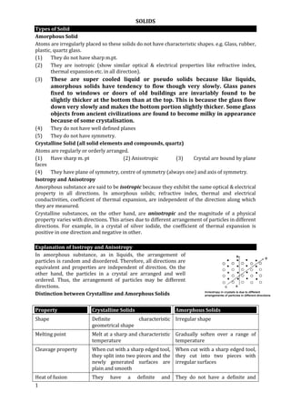
  • 1. SOLIDS 1 Types of Solid Amorphous Solid Atoms are irregularly placed so these solids do not have characteristic shapes. e.g. Glass, rubber, plastic, quartz glass. (1) They do not have sharp m.pt. (2) They are isotropic (show similar optical & electrical properties like refractive index, thermal expansion etc. in all direction). (3) These are super cooled liquid or pseudo solids because like liquids, amorphous solids have tendency to flow though very slowly. Glass panes fixed to windows or doors of old buildings are invariably found to be slightly thicker at the bottom than at the top. This is because the glass flow down very slowly and makes the bottom portion slightly thicker. Some glass objects from ancient civilizations are found to become milky in appearance because of some crystalisation. (4) They do not have well defined planes (5) They do not have symmetry. Crystalline Solid (all solid elements and compounds, quartz) Atoms are regularly or orderly arranged. (1) Have sharp m. pt (2) Anisotropic (3) Crystal are bound by plane faces (4) They have plane of symmetry, centre of symmetry (always one) and axis of symmetry. Isotropy and Anisotropy Amorphous substance are said to be isotropic because they exhibit the same optical & electrical property in all directions. In amorphous solids; refractive index, thermal and electrical conductivities, coefficient of thermal expansion, are independent of the direction along which they are measured. Crystalline substances, on the other hand, are anisotropic and the magnitude of a physical property varies with directions. This arises due to different arrangement of particles in different directions. For example, in a crystal of silver iodide, the coefficient of thermal expansion is positive in one direction and negative in other. Explanation of Isotropy and Anisotropy In amorphous substance, as in liquids, the arrangement of particles is random and disordered. Therefore, all directions are equivalent and properties are independent of direction. On the other hand, the particles in a crystal are arranged and well ordered. Thus, the arrangement of particles may be different directions. Distinction between Crystalline and Amorphous Solids Property Crystalline Solids Amorphous Solids Shape Definite characteristic geometrical shape Irregular shape Melting point Melt at a sharp and characteristic temperature Gradually soften over a range of temperature Cleavage property When cut with a sharp edged tool, they split into two pieces and the newly generated surfaces are plain and smooth When cut with a sharp edged tool, they cut into two pieces with irregular surfaces Heat of fusion They have a definite and They do not have a definite and
  • 2. SOLIDS 2 characteristic heat of fusion characteristic heat of fusion. Anisotropy Anisotropic in nature. Mechanical strength, electrical & properties changes with direction Isotropic in nature. Mechanical strength, electrical & optical properties are same in all direction. Nature True solids Pseudo solids or super cooled liquids Order in arrangement of constituent particles Long range order Only short range order Long range and short range : If in a solid, arrangement of particles follows regular and periodic pattern for short distance only it is called short range order and if regular and periodic pattern is observed in whole crystal its called long range order. Classification of Crystalline Solid: Type of Solid Constituent Particles Nature of Forces Examples Characteristics Properties 1. Ionic Positive and negative ions Strong electrostatic forces of attraction NaCl, KNO3, LiF, MgO Hard, brittle, high melting points (~ 1500 K), soluble in polar solvents, insulator in the solid state, good conductor in the molten state or aqueous solution. 2. Molecular Molecules 1.Non polar molecular solid- vander Waal’s forces 2.Hydrogen bond mol solid 3. Polar mol solid- dipole dipole interaction l2, Cl2, solid CO2 (dry ice), and Ar, CH4, Napthalene, glucose sulphur, ice Solid SO2, solid NH3 Soft, low melting points, low density, volatile and insulators of heat and electricity. 3. Network or Covalent Atoms Covalent bonds C (Diamond and graphite), Si, SiO2, SiC Boron, Black Very hard with very high melting point (~ 4000 K) and insulators (except graphite) 4. Metallic Atoms Metallic bond i.e. Attraction between positive metal ions (kernels) and mobile electrons All metals and some alloys Range from soft to very hard, high melting points (~ 800 – 1000 K) malleable and ductile, possess lustre, good conductors of heat and electricity. Explanation for the Metallic Properties The different physical properties of the metals mentioned earlier can be explained with the help of electron sea model for the metallic bonds. These are disused as follows: 1. Electrical Conductivity According to electron sea model, the electrons present in the sea are mobile but their movement is not systematic. When a potential difference is applied by placing electrodes on both sides of a metal, the movement of the electrons becomes systematic. They flow from cathode to the anode. As a result, the electrical current flows across a metal or it becomes conducting. The electrical conductivity of metals decreases with the rise in temperature. Actually when temperature increases, the average kinetic energy of the positively charged kernels
  • 3. SOLIDS 3 also increases. They start moving in the electron sea and obstruct the movement of the electrons leading decreased electrical conductivity. 2. Thermal conductivity When we heat a certain portion of a metal the kinetic energy of the electrons present increases. They move towards the colder regions and collide with the electrons with less kinetic energy. As a result, kinetic energy is transferred. Thus, heat is conducted through the metal . 3. Malleability and ductility We know that the metals are malleable (can be beaten into sheets) and ductile (can be drawn into wires). Both these characteristics can be explained with the help of electron sea model. When stress is applied on the metal surface, the kernels present in a particular layer slip over the other layer. The crystal lattice or the shape of the crystal gets deformed as a result of it. However, the environment of the kernels remains the same i.e. mobile electrons keep on attracting the kernels. Only there is a shift in the position of the kernels from the one lattice site to the other. 4. Metallic Lustre Metals have generally a shining surface known as lustre. This lustre is also due to the mobile electrons. When light falls on the surface of a metal, the electrons absorb photons and start vibrating at a frequency equal to that of the incident light. These vibrating electrons emit electromagnetic radiations in the form of light. As a result, the metal surface acquires a shining appearance known as lustre. 5. High tensile strength This is the property of the metal as a result of which they can be stretched without breaking. The tensile strength is because of strong electrostatic force of attraction between the kernels and mobile electrons. 6. Hardness of metals The hardness of metals is related to the strength of the the metallic bonds between the kernels and the mobile electrons. Greater the number of these electrons, stronger will be the bond. Similarly, smaller the size of the kernels, greater will be their attraction for the electrons. For example, sodium is very soft because the size oif the kernel is large and there is only one valence electron. Q. Why solids are hard and rigid? A. Solids are hard and rigid because the intermolecular distances between solids are very less and the intermolecular forces operating between the molecules are very strong. Thus the molecules in solids are packed very close to each other. Hence they cannot move about freely and can only vibrate about their positions. Q. Why solids have definite volume? A. Any matter that is a solid has a definite shape and a definite volume. The molecules in a solid are in fixed positions and are close together. Although the molecules can still vibrate, they cannot move from one part of the solid to another part. As a result, a solid does not easily change its shape or its volume. Q. Ionic solids are hard and rigid in nature? A. In ionic crystal the lattice is made of positive and negative ions. These are held together by ionic bonds – the strong electrostatic attractions between oppositely charged ions. Consequently, the cations and anions attract one another and pack together in an arrangement so that the attractive forces maximize. Each ion is surrounded by neighbours of opposite charge and there are no separate molecules. Since the ions are fixed in their lattice sites, typical ionic solids are hard and rigid with high melting points. Q. Ionic solids are brittle?
  • 4. SOLIDS 4 A. On hammering or applying stress a layer of ions slips away from their oppositely charged neighbours and brings them closer to ions of like charge. The increase of electrostatic repulsions along the displaced plane causes the crystal to break. Space Lattice and Unit Cell Space Lattice: The geometrical form consisting only of a regular array of points (atoms, molecules, ion) in space is called space lattice or it can be defined as an array of points showing how molecules, atoms or ions are arranged in different sites in three dimensional space. The sites which are occupied by constituent units (molecules ions or atoms) are called lattice points. Unit Cell: It is defined as the smallest building block of a solid which when repeated over and again results into the space lattice. We must specify the unit cell by length of its edges and the angles between them. Parameters of a unit cell: A unit cell is characterized by : (i) Its dimensions (lengths) along the three edges as ‘a’, ‘b’ and ‘c’. These edges may or may not be mutually perpendicular. (ii) Angles ,  and  between the pair of edges. The angle  is between the edges b and c, angle  is between the edges c and a and angle  is between the edges a and b. Thus, a unit cell is characterized by six parameters, a, b, c, ,  and . IMPORTANT unit cell: Cubic cell a = b = c  =  =  = 90o Monoclinic a  b  c  =  = 90o   90o Hexagonal a = b  c  =  = 90o, Triclinic a  b  c       90o Note : Cubic is the most stable and symmetrical while triclinic least stable and unsymmetrical. Types of unit cell: i) Primitive or simple unit cell When a unit cell contain constituent particles only at corners ,it is called primitive unit cell ii) Non –Primitive unit cells When a unit cell contain one or more constituent particles at corners & some other positions. It is called centered unit cell. There are three types non–primitive unit cell e.g. i) Body centred : – When lattice points are at corners & centre of unit cell.
  • 5. SOLIDS 5 ii) Face centred: – When lattice points are at corners & centre of each face of unit cell iii) End centred: – When lattice points are at corners & centre of two opposite faces. Effective Number of Atoms Per Unit Cell (Rank of Unit Cell) 1. Atom at the corner of unit cell is shared by 8 unit cells. Thus, contribution of each corner atom (per unit cell) is 1/8. 2. Atom present at the face of a unit cell is shared by 2 unit cells. Contribution of face atom (per unit cell) is 1/2. 3. For atom present at the centre of unit cell, contribution per unit cell is equal to 1. 4. For atom present at the edge of unit cell is shared by 4 unit cells. Contribution of edge atom (per unit cell) is 1/4. (1) Rank for Cubic Unit Cell It is the effective number of atoms present in cell. It is represented by Z. nc = no. of corner atoms, nf = no. of face atoms nb = no. of body atoms (inside the cube) ne = no. of edge atoms Rank = b efC n 4 n 2 n 8 n  for cubic unit cell Assignment – I Q.1 A compound formed by elements X and Y crystallizes in the cubic structure where Y atoms are at the corners of the cube and X atoms are at the alternate faces. What is the formula of the compound? Q.2 If three elements P, Q and R crystallize in a cubic solid lattice with P atoms at the corners, Q atoms at the cube centre and R atoms at the centre of the faces of the cube, then write the formula of the compound. Q.3 Potassium crystallizes in a body–centred cubic lattice. Calculate the approximate number of unit cells in 2g potassium. Atomic mass of potassium  39u. Q.4 In a face centred lattice of X and Y, X atoms are present at the corners while Y atoms are at face centres. Then the formula of the compound if one of the X atoms is missing from a corner in each unit cell would be: (a) X7Y24 (b) X24Y7 (c) XY24 (d) X24Y
  • 6. SOLIDS 6 Packing of Spheres in Solids: (A) Close Packing in One Dimension Close packing of spheres in one dimension. (B) Close Packing in Two Dimensions (b) Three dimensional close packing from two dimensional hexagonal close packed layers In the first layer there are some empty spaces or hollows called voids. These are triangular in shape. These triangular voids are of two types marked as a and b. All the hollows are equivalent but the spheres of second layer may be placed either on hollows which are marked a or on other set of hollows marked b. It may be noted that it is not possible to place spheres on both types of hollows. Let us place the spheres on hollows market b to make the second layer which may be labeled as B layer. Obviously the holes marked ‘a’ remain unoccupied while building the second layer. Whenever a sphere of second layer is placed above the void of first layer, a tetrahedral void is formed. These voids are called tetrahedral voids because a tetrahedral is formed when the centres of these four spheres are joined. There are marked at ‘T’ voids. The voids ‘a’ are double triangular voids. The triangle void in the second layer are above the triangular voids in the first layer and the triangular shapes of these voids do not overlap. One of them has the apex of the triangle pointing upward & other downward. Such voids are surrounded by six spheres and are called octahedral voids. Now the third layer can be build up by placing spheres above tetrahedral voids or octahedral voids.
  • 7. SOLIDS 7 (II) Placing Third Layer over the Second Layer: When third layer is placed over the second, there are two possibilities. (a) Covering tetrahedral voids When a third layer is to be added, again there are two types of void available. One type of void marked ‘a’ are unoccupied hollows of the first layer. The other type of void are void in the second layer (marked c). Thus, there are two alternative to build the third layer. Tetrahhedral Void Octahedral Void
  • 8. SOLIDS 8 Solid Circle Represent Layer A and Dotted Actual view of hexagonal close packing Circle Represent Layer B The third layer of sphere may be placed on the tetrahedral voids marked (c) of the second layer. In this arrangement, the spheres of the third layer lie directly above those in the first layer. In other words, third layer becomes exactly identical to the first layer (labelled A). As shown in figure. Simplified view of Hexagonal close packing (AB AB …… pattern) This type of packing is referred to as ABABA …. arrangement. This type of packing is also known as hexagonal close packing. This type of arrangement is found in many metals like Mg and Zn. (b) Covering octahedral voids The second way to pack spheres in the third layer is to place them over octahedral voids marked ‘a’ (unoccupied void of first layer). This gives rise to a new layer labeled as C. Sphere of third layer are not alligned with first layer or second layer. However, it can be shown that the spheres in the fourth layer will correspond to those in the first layer. As shown in figure.
  • 9. SOLIDS 9 This type packing is called as the ABCABCA ….. type of arrangement. It is also known as cubic close packing( ccp) or face centred cubic arrangement (fcc). It may be noted that both types of packing are equally economical though these have different forms. In both cases, 74% of the available volume is occupies by the spheres and co–ordination no equal to12 . Metals like Cu & Ag crystallies in FCC pattern. (c) Body centred cubic close packing (ABAB …. Type) Co–ordination No. = 8 In this packing atom of each layer will not touch any other atom of the same layer but four atoms of one layer will touch to same atom of second layer. In this packing unit cell will be BCC and arrangement of first and third layer will be same Important facts about Unit cells and the Packing of Spheres in Crystalline Solids (i). Particles pack together in crystals so that they can be as close together as possible to maximize intermolecular attractions. (ii). Simple cubic packing – the spheres in one layer sit directly on top of those in the previous layer. (AAA……) 1. All layers are identical having both vertical and horizontal alignment of atoms. 2. Primitive – cubic unit cell. 3. Coordination number = 6. Sphere touches four neighbours in the same layer, one above and one below. 4. Uses only 52% of available volume. (iii). Body – centered cubic packing – spheres are in alternate layers in an ABAB….. arrangements where the spheres in the B layers fit into the small depressions between spheres in the neighbouring layers. Atoms of each layer will not touch to each other but four atoms of same layer will touch to same atom of 2nd layer. 1. Body – centered cubic cell.
  • 10. SOLIDS 10 2. Coordination number = 8; four neighbours above and four neighbours below 3. Occupies 68% of the available volume. 4. S–Block elements forms BCC unit cell (iv). Hexagonal close packing– noncubic unit cell with two alternating layer (ABAB……) 1. Hexagonal arrangement of touching spheres. 2. Spheres in B layer fit into the small triangular depressions between spheres of A layer. 3. Coordination number = 12 4. Six neighbours in the same layer, three above and three below. (v). Cubic close packing– face centered cubic unit cell with three alternating layers, (ABCABC …...) 1. A – B layers identical to hexagonal close packing 2. Third layer is offset from both A and B. 3. Co–ordination number 12 4. Transition metal forms FCC unit cell (vi) Cubic is the most symmetrical while triclinic is the most unsymmetrical system. (vii). Sr. No. Structure Type of packing Stacking pattern Coordinatio n number Space used (%) Unit cell (a) Simple cubic Square close packing AAA … 6 52 Primitive cubic (b) Body centred cubic Square close packing ABAB….. 8 68 Body centred cubic (c) Hexagonal close packed Hexagonal ABAB… 12 74 (Non–cubic) (d) Cubic close packed Hexagonal ABCABC… 12 74 Face centred cubic (viii) In FCC or CCP there are three different layers which are constantly repeated in three dimensions. In HCP every first & third layers are same and in ccp every first & fourth layers are same. Between A & B (in close packing) the Octahedral & tetrahedral voids are located. If we place atoms of 3rd layer over the tetrahedral void, the layer A will be repeated, hence ABAB….. structure or HCP will be formed. If we place atoms of third layer over Octahedral void, then FCC will be generated as third layer will be different layer & it is ABCABC ….. type. The number of nearest neighbours for any atom, molecule or ion in a space lattice is called the coordination number. Type of Cubic Unit Cell & Packing Fraction 1. Simple or Primitive Cubic Unit Cell:
  • 11. SOLIDS 11 2. Body–Centred Cubic Unit Cell (BCC Unit Cell) 3. Face centred Cubic Unit Cell (FCC Unit Cell) Radius Ratio for the octahedral void under ideal condition.
  • 12. SOLIDS 12 Radius Ratio of Tetrahedral Void Body diagonal of smaller cube & larger cube are collinear & body diagonal of smaller cube is exactly half the larger cube. Body diagonal of smaller cube = 2 1 × Body diagonal of larger cube cubeerarglofdiagonalBody 4 1 rr ac  a3 4 1 rr ac  ….. (1) In FCC unit cell 4ra = a2 …… (2) from (1) & (2) aac r 2 3 rr  1 2 3 r r a c  = 0.225 Thus, for an atom to occupy a tetrahedral void, its radius must be 0.225 times the radius of the sphere Radius Ratio Rules For the stability of an compound, each cation should be surrounded by maximum number of anions and vice versa (for maximum electrostatic forces of attraction). The number of oppositely charged ions surroundings each ions is called its co–ordination number. Since ionic bond is non–directional, the arrangement of ions within the ionic crystal is determined by the sizes of the ions. The ratio of the radius of the cation to that of the anion is called radius ratio, i.e. atomhostofRadius atomquestofRadius )r(aniontheofRadius )r(cationtheofRadius RatioRadius a c  The guest atom must make a contact with host atom but host atom may or may not make contact. Evidently, greater is the radius ratio, the larger is the size of the cation and hence greater is its co–ordination number. The relationships between the radius ratio and the co– ordination number and the structural arrangement are called radius ratio rules, and are given in Table. Radius ratio rules for AB type structures Radius Ratio Co– ordination no Structural arrangement Structure type Examples =0.155 but < 0.225 3 Planar triangular – B2O3 =0.225 but <0.414 4 Tetrahedral Sphalerite, ZnS CuCl, CuBr, Cul, BaS =0.414 but < 0.732 6 Octahedral Sodium chloride (Rock salt) HgS, NaBr, KBr, MgO, MnO, CaO, CaS =0.732 but <1.0 8 Body–centred cubic Caseium chloride Csl, CsBr, TlBr, NH4Br The increase in coordination number with increase in radius ratio can be easily understood by considering a particular cation (so that its size i.e. r+ remains constant) and arranging anions of decreasing size around it (so that r– decreases and hence r+/r– increases). We observe that as the radius ratio increases, the number of anions touching the cation increases i.e. coordination number increases
  • 13. SOLIDS 13 Illustrating effect of radius ratio on co–ordination number. As rc/ra increases, coordination number increases Q. 1 Atoms of element B from hcp lattice and those of the element A occupy 2/3rd of tetrahedral voids. What is the formula of the compound formed by these elements A and B? Q.2 In a crystalline solid, anions B are arranged in a cubic close packing. Cations A are equally distributed between octahedral and tetrahedral voids. If all the octahedral voids are occupied, what is the formula of the solid? Q.3 In the mineral, spinel, having the formula MgAl2O4, oxide ions are arranged in the cubic close packing, Mg2+ ions occupy the tetrahedral voids while Al3+ ions occupy the octahedral voids. (i) What percentage of tetrahedral voids is occupied by Mg2+ ions? (ii) What percentage of octahedral voids is occupied by Al3+ ions? Q.4 In a solid oxide ions are arranged in cubic close packing. One-sixth of the tetrahedral voids are occupied by cations A while one-third of the octahedral void are occupied by the cations B. What is the formula of the solid? Q.5 B– ions form a close packed structure. If the radius of B– ion is 195 pm, calculate the radius of the cation that just fits into the tetrahedral hole. Can a cation A+ having a radius of 82 pm be slipped into the octahedral hole of the crystal A+ B–? Q.6 If the close packed cations in an NaCl type solid have a radius of 75 pm, what would be the maximum and minimum sizes of the anions forming the voids? Density of Cubic Unit Cell In NaCl type unit cell, d = rc + ra = a/2 In CsCl type d = rc + ra = a 2 3 [2d = Body diagonal] In ZnS type 4ra = a2 Q.1 CsCl has cubic structure. Its density is 4.0g cm–3. What is the distance between Cs+ and Cl– ions? (At. mass of Cs = 133) 357 pm
  • 14. SOLIDS 14 Solid defect Electronic imperfecton Atomic imperfection (Point defect) Stoichiometric defect If number of cation & anion remain same after the defect so stoichiometry will be preserved Non stoichiometric defect No. of cation & anion ratio changes so stoichiometry is distrubed by this defect Impurity defect Schottky defect Frenkel defect Due to deficiency of metal Due to excess of metal Interstitial if impurity atoms are small Substitutional if impurity atoms are of same size as that of host atoms Due to presence of extra metal ions Due to anion vacancies (F - centre) Q.2 An element has a body–centred cubic (bcc) structure with edge of 288 pm. The density of the element is 7.2g/cm3. How many atoms are present in 208g of the element? 24.17 × 10²³ atoms Q.3 KF has NaCl structure. If the distance between K+ and F– is 269 pm, find the density of KF(NA = 6.02  1023 mol–1, atomic masses K = 39, F = 19 amu). 2.48 gm/cm3 Q.4 Calculate the density of silver which crystallizes in a face–centred cubic structure. The distance between the nearest silver atoms in this structure is 287 pm. (Molar mass of Ag =107.87g mol –1, NA = 6.02  1023 mol–1) 10.71 gm/cm3 Q.5 The density of a face centred cubic element (atomic mass = 60.2 amu) is 6.25g cm–3. Calculate the length of the edge of the unit cell. 4 × 10⁻⁸ cm Q.6 What is the distance between Na+ and Cl– in a NaCl crystal if its density is 2.165g cm–3? NaCl crystallizes in the fcc lattice. 281 pm Defect in Solid Ionic crystals can have perfect arrangement only at absolute zero temperature. According to third law of thermodynamics, S = 0 only at 0 K. At any temperature above 0 K, the crystals have some departure from complete ordered arrangement. With increase of temperature S will increase so G will becomes more negative (G = H – TS). Even single crystals which are grown with all care and which appear to be perfect may contain some internal irregularities. So the process of defect formation will become more prominent. Hence solid defect is a natural phenomenon. Any deviation from completely ordered arrangement in a crystal constitutes a disorder or a defect. The crystal may have defects due to the presence of some impurities. 1. Electronic Imperfection These correspond to defects due to the electrons. In perfect crystal at 0 K electrons are present the fully occupied lowest energy states. But at higher temperature (above 0 K), some of the electrons may occupy higher energy states, depending upon the temperature. These electrons become free to move and therefore, they are responsible for the electrical conductivity. The atom from which electrons have been removed become electron deficient and these are referred to as holes. The holes also give rise to electrical conductivity, but the direction of motion of holes in an electric field is opposite to that of
  • 15. SOLIDS 15 the electrons. Free electrons and holes in crystals are considered to be electronic imperfections. These electronic imperfections are responsible for electrical conductance. 2. Point Defect If atoms are missing from lattice point, displaced or extra ions are present, it is called point defects [electrical neutrality of the crystal is never affected by any kind of defect]. There are three types of point defects (a) Stoichiometric defect (b) Non–stoichiometric (c) Impurity defects (A) Stoichiometric defect: In which stoichiometry of crystal is maintained even after the defect. i.e. Number of positive & negative ions are exactly in the same ratios as in non–defected solids. (i) Schottky defect It is basically a vacancy defect in ionic solid. When a crystal site become vacant by removal of a structural unit in the lattice, then the defect is referred to as the vacancy defect. In an ionic crystal, a cation and anion may leave the lattice to cause two vacancies. Such a defect which involves equal no of cation and anion vacancies in the crystal lattice is called a schottky defect. Cation vacancy is followed by anion vacancy leading to decrease in density. Compound with high Co. no. & high ionic character shows this defect. The crystal begins to conduct electricity to a smaller extent by ionic mechanism. The stability of the crystal is lowered. e.g. NaCl, CsCl. It has been observed that in NaCl, there are about 106 Schottky pair per cm3. In 1 cm3 there are about 1022 ions. Thus there is one schottky defect per 1016 ion. (ii) Frenkel Defect This defect is shown by ionic solids. The small ion (usually cation) is dislocated from its normal site to an interstitial site. It creates a vacancy defect at its original site & an interstitial defect at its new location. Small ions are displaced from their standard lattice point and present in non–standard lattice points i.e. interstitial. This is also called dislocation defect. It does not change the density of the solid as atoms are not absent from lattice they are just displaced. This defect is shown by those ionic solids in which there is a large difference in size of ions and low co.od(less ionic character] e.g. Zng, AgCl, Agl, AgBr due to presence of small Zn+2 and Ag+ . AgBr shows both Schottky and Frenkel defect. (It is because AgBr crystal has a coordination number of 6 which is neither high nor low. The radius ratio of AgBr is also intermediate, thus AgBr satisfies the conditions to exhibit both type of defects.) Consequences of Schottky and Frenkel Defect Schottky & Frenkel defects in crystals lead to some interesting consequences. These are given below: 1. Because of the presence of these defects, the electrical conductivity of crystal increases. When an electric field is applied, a nearby ion moves from its lattice site to occupy a ‘hole’. This results in creating a new ‘hole’ and another nearby ion moves into it and so on. This process continues and hole, thereby, move from one end to the another end. Thus, it conducts electricity across the whole of the crystal.
  • 16. SOLIDS 16 2. Due to the presence of holes in the crystal, its density decreases. However it may be noted that density decreases only for crystals having Schottky defects. 3. The presence of ‘holes’ also decreases the lattice energy or the stability of the crystal. The presence of too many holes may cause a partial collapse of the lattice. B. Point Defects in Non–Stoichiometric Crystals The compounds in which the ratio of positive and negative ions present in the compound differs from that required by ideal chemical formula of the compound are called non– stoichiometric compounds. The defects in these compounds are called non– stoichiometric defects. These are of two types depending upon whether positive ions are in excess or negative ions are in excess. These are also known as metal excess defects and metal deficiency defects respectively. (A) Metal Excess Defects In these defects, the positive ions are in excess. These may arise due to the following two ways: (i) Anion vacancies In this case, negative ions may be missing from their lattice sites leaving holes in which the electrons remain entrapped to maintain the electrical neutrality. Evidently, there is an excess of positive (metal) ions although the crystal as a whole is electrically neutral. This type of defect is observed in those crystals which are likely to form Schottky defects. For example, in alkali metal halide, anion vacancies are produced when alkali metal halide crystals are heated in the atmosphere of the alkali metal vapours. The metal atoms get deposited on the surface of the alkali metal halide crystal, halide ions move into the surface and combine with metal atoms. The electrons, thus produced by the ionization of the metal atoms diffuse into the crystal and get trapped at the anion vacancies. The electrons trapped in anion vacancies are referred to as F–centre (from German word farbe centre for colour centre). These give very interesting colours. For example (i)LiCl crystal appear pink when heated in presence of Li vapours.. (ii)NaCl crystal appear yellow when heated in presence of Na vapours. (iii)KCl crystal appear pink when heated in presence of K vapours. (ii) Excess cations occupying interstitial sites In this case, there are extra positive ions occupying interstitial sites and the electrons in another interstitial sites to maintain electrical neutrality. This type of defect is found in crystals which are likely to develop Frenkel defect. The common example is zinc oxide. Zinc oxide (ZnO) loses oxygen reversibly at high temperatures and turns yellow in colour. The excess Zn2+ ions are trapped in interstitial sites and equal number of electrons are trapped in the neighbourhood to balance the electrical charge. There is excess of zinc in the crystal and its formula becomes Zn(1 + x) O. These free electrons are responsible for conductance. This is the only defect where density increases. 2 2 O 2 1 e2ZnZnO   Electron remains trapped in Anion vacancy (F – centre)
  • 17. SOLIDS 17 Consequences of Metal Excess Defects 1. The crystal with metal excess defects conducts electricity due to the presence of the electrons. These compounds are also called n–type semi–conductors since the current is carried by the electrons in the normal way. 2. The crystals with metal excess defects are generally coloured. For example, non– stoichiometric sodium chloride is yellow, non–stoichiometric potassium chloride is violet. (B) Metal Deficiency Defects There are many solids which are difficult to prepare in stoichiometric composition and contain less amount of the metal as compared to the stoichiometric proportion. Mostly this happens with transition metal salts. e.g. FeO which is mostly found with a composition of Fe0.95O. It may actually range from Fe0.93O to Fe0.95O. In crystals of FeO some Fe+2 cations are missing and the loss of positive charge is made up by the presence of required number of Fe+3 ion. Three ferrous ions are replaced by two ferric ions to maintain electrical neutrality, so one cation vacancy is produced. Average oxidation number of iron will be more than 2 but less than 3. When the low valency cation changes into high valency cation, then cationic vacancies are produced. Concentration of cation vacancy is the number of cations vacancy present in 1 mole of dopped crystal. e.g. In Fe0.92O one mole of compound will have 0.08 moles of cation vacancy and will have 0.16 mole of Fe+3 ion so the number of vacancy will be 0.08 × 10²³. OR
  • 18. SOLIDS 18 It can be calculated by balancing net positive and negative charge. If x mole of Fe+3 ions are present then moles of Fe2+ will be (0.92 – x) mole net positive charge = net negative charge 3x + (0.92 – x) 2 = 2 3x + 1.84 – 2x = 2 x = 2 – 1.84 = 0.16 Number of cation vacancy = 0N 2 x  = 0.08 × N0 (C) Impurity defects(Doping) These defects are due to presence of foreign particles in host atoms. (i) Substitutional Impurity defect (in ionic compounds) If impurity atoms have same size as that of host atoms, they will replace host atom. If valency of impurity atom is more than host atom some of the host cation will leave the crystal to maintain electrical neutrality thus some cation vacancy will create in the crystal to form a non–stoichiometric compound e.g. impurity of CdCl2 in NaCl. Number of cation vacancy is some as that of Cd+2 ion but if there is impurity of AlCl3. Number of vacancy will be double than the number of Al+3 (ii) Impurity Defects in Covalent Compound The impurities are of two types: (i) Donors (Electron rich impurities) (ii) Acceptors. (Electron deficient) (i) Electron rich impurities Let us consider that some atoms with five valence electrons (donors) such as arsenic (As) are added to the germanium crystal. A minute proportion of Si atoms are randomly replaced by ‘As’ atoms with five electrons in their outermost shell. Ge atom is substituted by an atom of As, four the electrons in arsenic form covalent bonds with surrounding Ge atoms and the fifth electron remains free. Hence, an extra electron, over and above the number required for forming the four covalent bonds, gets introduced in the crystal. This extra electron which is not needed for bonding become delocalized and can serve to conduct electricity and therefore, germanium containing traces of arsenic (or arsenic doped germanium) exhibit electrical conductivity. This type of conduction is known as n–type semiconduction where ‘n’ stands for negative because electron are responsible for semiconducting behaviour. This is shown in figure. Doping of a germanium or silicon with other group–15 elements such as P, Sb or Bi also given n–type semiconductors. (ii) Electron deficit Impurities An acceptor impurity helps in conduction in the following way. Suppose some atoms of germanium are doped with acceptor atoms having only three outer shell electrons such as indium. Each indium
  • 19. SOLIDS 19 atom uses its three electrons to form three bonds to complete the network structure of Ge. As a result, some sites normally occupied by electrons will be left empty and gives rise to electron deficiencies. The electron deficiency sites are called electron vacancies or positive holes(hypothetical). Thus doping the germanium with traces of indium increases the electrical conductivity of the germanium crystal. This type of conduction is called p–type semiconductor because holes (positive in charge appears to be responsible for the semi-conducting properties. Doping of silicon or germanium with other group–13 elements such as B, Al or Ga give p– type semiconductors. Distinction between n–type Semiconductors and p–types Semiconductors n–type Semiconductor p–types Semiconductor 1. It is an extrinsic semiconductor which is obtained by doping the impurity atoms of 15th group of periodic table to the pure germanium or silicon semiconductor. 1. It is an extrinsic semiconductor which is obtained by doping the impurity atoms of 13th group of periodic table to the pure germanium or silicon semiconductor. 2. The impurity atoms added, provided extra electrons in the structure, and are called donor atoms. 2. The impurity atoms added, create vacancies of electrons (i.e. holes) in the structure and are called acceptor atoms 3. The electrons are majority carries and holes are minority carriers 3. The holes are majority carriers and electrons are minority carriers. Binary Solid Silicon and Germenium of group 14 elements have characteristic valency four & form four bonds as in diamond. Solid binary compounds other than Si and Ge are prepared by combining elements of two such groups so that they will have an average valence of 4. These are called compounds of group 12–16 and 13–15 e.g. of 12–16 compounds = ZnS, CdS, CdSe, HgTe 13–15 compounds = lnSb, AlP, GaAs. In these compounds, the bonds are not perfectly covalent and the ionic character depends upon the electronegativity difference between the two elements. Properties of Solids 1. Electrical Properties of Solids On the basis of electrical conductivity, solids can be classified into three types: (i) conductors (ii) semi–conductors (iii) insulators The conductivity of a solid is one of its characteristic properties and throws light on the internal structure and bonding in the solid. Electrical conductivity of metals is very high and is of the order of 104 to 107 –1 m–1. The insulators, on the other hand, have conductivity in the range of 10–10 to 0–20 –1 m–1. Semiconductors have intermediate conductivity which is in range 10–6 to 104 –1 m–1. (i) Conductors The solids which allow the passage of electric current are called conductors. These are of two types: metallic conductors & electrolytic conductors. (a) Metallic Conductors
  • 20. SOLIDS 20 Metallic conductors are those which allow the electricity to pass through them without undergoing any chemical change. For example, copper, silver etc. In metallic conductors, the conductance is due to the movement of electrons under the influence of an applied electric potential. The steams of electrons constitute the current. Metals conduct electricity in solid as well as in molten state. The conductivity of metal depends upon the number of valence electrons available per atom. The atomic orbitals of metal atoms form molecular orbitals, which are so close in energy to each other as to form a band. If this band is partially filled or it overlaps with a higher energy unoccupied conduction band, then electron can flow easily under an applied electric field and metal shows conductivity. (ii) Insulators The solids which do not allow passage of electric current through them are called insulators. For example, wood, sulphur, phosphorus, rubber, etc. The gap between valence band and conductor band is large, so electron cannot jump to it. (iii) Semi–conductors The solids whose conductivity lies between those of typical metallic conductors and insulators are called semi–conductors. The semi–conductors have conductivity in the range of 10–6 to 104 –1 m–1. The gap between valence band and conduction band is small. Therefore some electrons may jump to conduction band and show some conductivity. Electrical conduction can be increased by increasing temperature since more electron can jump to conduction band. Si and Ge shows this behaviour and are called intrinsic semiconductor. The conductance of these intrinsic semiconductor is too low to be of practical use. Their conductance can be increased by adding an approximate impurity. (Doping means the introduction of small amounts of impurities like phosphorous, arsenic or boron into the pure crystal). The conductivity of silicon and germanium increase drastically by doping it with certain other elements. Mechanism of Electrical Conduction In metals, conductivity strongly depends on the number of valence electrons available per atom. The difference is electrical conductance behaviour of conductors, insulators and semiconductors can be explained with the help of band model. It is based on the molecular orbital theory. The basis of band model is that a metal lattice has an extremely large number of atoms. The atomic orbitals of metal atoms form a large number of molecular orbitals which are so close in energy to each other that they form a band. If the band is partially filled or it overlaps with a higher energy unoccupied band, then electrons can easily flow under an applied electric field and metal shows conductivity. For example, a partially filled band is shown in figure (a) and overlapping bands are shown in figure (b) found in metals. Therefore, when some electric field is applied electrons can easily move within partially filled band or empty overlapping and this movement is responsible for electrical conductance of the substance. This type of behaviour is shown by metals.
  • 21. SOLIDS 21 Distinction between metals, insulators and semiconductors in. terms of band theory The spaces between valence band and conduction band represent energies forbidden to electrons and are called energy gaps or forbidden zone. The valence band and conduction bands for metals, semi–conductors and insulators are shown in figure. (i) In metals, the conduction band is close to valence band and therefore, the electrons can easily go into the conduction band. Therefore, metals are good conductors. (ii) In insulators, we energy gap between valence band and conduction band is very large. Therefore, the empty bands are not accessible for conduction and therefore, electrons from valence band cannot move into the conduction band. (iii) Several solids have properties intermediate between metals and insulators. These are called semi–metals or semi–conductors. They have only small difference in energy between the filled valence band and empty conduction band. If the crystal were cooled to absolute zero, the conduction band would be empty possible energy levels. The material would be a perfect insulator. However at ordinary temperature some electron are thermally excited from valence band to the conduction band and hence they can conduct electricity by the passage of electrons at normal temperatures. The conductivity is in between that of a metal and an insulator and depends upon the number of electrons in the conduction band. Distinction between Intrinsic and Extrinsic Semiconductor Intrinsic Semiconductor Extrinsic Semiconductor 1. It is pure semiconducting material and no impurity atoms are added to it. 1. It is prepared by doping a small quantity of impurity atoms to the pure semiconducting material 2. Examples are crystalline forms of pure silicon and germanium 2. Examples are silicon and germanium crystals with impurity atoms of arsenic, antimony, phosphorous etc. or indium, boron, aluminum etc. 3. The number of free electrons in conduction band and the number of holes in valence band is exactly equal to very small indeed. 3. The number of free electrons and holes is never equal. There is excess of electron in n–type semiconductors & excess of holes in p–type semiconductors. 4. Its electrical conductivity is low. 4. Its electrical conductivity is high. 2. Magnetic Properties of Solid Every substance has some magnetic properties associated with it. The origin of these properties lies in the electrons.
  • 22. SOLIDS 22 Each electron in an atom has magnetic moment which originates from two sources: (i) Orbital motion around the nucleus. (ii) Spin of electron around its own axis. A moving electron may be regarded as a small current loop generating a small magnetic field and having a magnetic moment along its axis of rotation as shown in figure (a). The magnetic field which originates from electron spin is directed along the spin axis. The spin magnetic moments are generally shown by up and down direction as shown in figure (b). Thus, each electron in an atom fundamental magnetic moment is the Bohr magneton B which is equal to 9.27 × 10⁻²⁴ A m2. For each electron in an atom, the spin magnetic moment is + B depending upon the two possibilities of the spin. Magnetic dipoles which may exist in a material can be analogous to electric dipoles. Magnetic dipoles may be thought of as small bar magnet composed of north and south poles instead of positive and negative electric charges. The magnetic properties of solids are also related to the electronic structures. Materials can be divided into the following types depending upon their response to magnetic field: (a) Diamagnetic Substances The substances which are weakly repelled by magnetic field are called diamagnetic substances. E.g. TiO2, NaCl. Diamagnetism arises when all the electrons are paired. Paring of electron cancels their magnetic field. (b) Paramagnetic Substance The substances which are weakly attracted by magnetic field are called paramagnetic substances. These substances have magnetic dipoles due to the presence of some species (atoms, ions or molecules) with unpaired electrons. The paramagnetic substances lose their magnetism in the absence of magnetic field. For example, TiO, VO2 and CuO. (c) Ferromagnetic Substances: The substances which are strongly attracted by magnetic field are called ferromagnetic substances. These substances show permanent magnetism even in the absence of magnetic field. Some examples of ferromagnetic solids are: iron, cobalt, nickel and CrO2. Ferromagnetism arises due to spontaneous alignment of magnetic moments of ions or atoms in the same direction. In solid state metal ions of ferromagnetic substance are grouped together into small regions called domains. Such domain act as magnet. When the substance is placed in a magnetic field. All the domains get oriented in the direction of magnetic field and strong magnetic effect is produced. In an unmagnetised piece of ferromagnetic substance the domain are randomly oriented and their magnetic moments get Schematic alignment of magnetic moments in (i) Ferromagnetic (ii) antiferromagnetic and (iii) Ferrimagnetic (i) (ii)
  • 23. SOLIDS 23 cancelled. The ordering of domain persists even when the magnetic field is removed and the ferromagnetic substance becomes a permanent magnet. (d) Antiferromagnetic Substances Alignment of magnetic moments in opposite direction in a compensatory manner and resulting in a zero magnetic moment (due to equal number of parallel and antiparallel magnetic dipoles) gives rise to antiferromagnetism. For example, MnO, Mn2O3 and MnO2 are antiferromagnetic. (e) Ferrimagnetic Substances: Alignment of magnetic moments in opposite directions resulting in a net magnetic moment (due to unequal number of parallel and anti–parallel magnetic dipoles) gives rise to ferri–magnetism. For example, Fe3O4 is ferromagnetic, ferrite Mg Fe2O4, ZnFe2O4. Ferromagnetic and ferrimagnetic substances change into paramagnetic substances at higher temperatures due to randomization of spins. Fe3O4, which is ferromagnetic at room temperature, becomes paramagnetic at 850 K. This temperature is called curie’s temperature. All the ferro, ferri and antiferro–magnetic substances get converted into paramagnetic state at some characteristic temperature. This happens because the temperature change effect the order of spins. For example, magnetite becomes paramagnetic at 850 K. Magnetic Properties of Solids Properties Description Alignment of Magnetic Dipoles Examples Applications 1. Diamagnetic Feedly repelled by the magnetic fields. Non–metallic elements (except O2, S) inert gases and species with paired electrons are diamagnetic All paired electron    TiO2, V2O5, NaCl, C6H6 (benzene) Insulator 2. Paramagnetic Attracted by magnetic field due to the presence of permanent magnetic dipoles (unpaired electrons). In magnetic field, these tend to orient themselves parallel to the direction of field and thus, produce magnetism in substances.    at least one unpaired electron O2, Cu2+, Fe3+, TiO, Ti2O3, VO, VO2, CuO Electronic appliances 3. Ferromagnetic Permanent magnetism even in the absence of magnetic field. Above a temperature called Curie temperature, there is no ferromagnetism. Dipoles are aligned in the same direction      Fe, Ni, Co, CrO2 CrO2 is used in audio and video tapes 4.Antiferromagnetic This arises when net dipole alignment is zero due to equal and opposite alignment.       MnO, MnO2, Mn2O, FeO, Fe2O3, NiO, Cr2O3, CoO ____ 5. Ferrimagnetic This arises when there is net dipole moment       Co3O4, Fe3O4, ferrities ____