
Recomendados
Más contenido relacionado
La actualidad más candente
La actualidad más candente (20)
Destacado
Destacado (18)
Similar a Emb day2 8051
Similar a Emb day2 8051 (20)
Último
Último (20)
Emb day2 8051
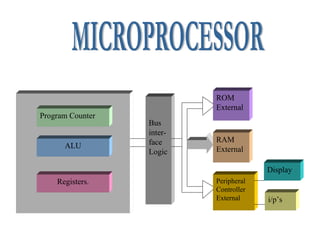
- 2. EXTERNAL INTRRUPTS INTERRUPT CONTROL ON-CHIP ROM FOR PROGRAM CODE TIMER0 ON-CHIP RAM TIMER1 COUNTER INPUTS CPU OSC BUS CONTROL 4 I/O PORTS P0 P1 P2 P3 ADDRESS/DATA SERIAL PORT TXD RXD
- 3. Microprocessor : •CPU is stand-alone, RAM, ROM, I/O, timer are separate •Designer can decide on the amount of ROM, RAM and I/O ports. •Expensive •Versatility •General-purpose Microcontroller: •CPU, RAM, ROM, I/O and timer are all on a single chip •Fix amount of on-chip ROM, RAM, I/O ports •For applications in which cost, power and space are critical •Single-purpose
- 5. Overview of 8051 family 8051 is a 8-bit micro controller ,it is introduced by Intel corporation.8051 is the original member of the 8051 family. Other members of 8051 family 8052 and 8031 are the other family members of 8051. The following table gives comparison of 8051 family members Feature 8051 8052 8031 ROM(on-chip program space in bytes) 4K 8K 0K RAM(bytes) 128 256 128 Timers 2 3 2 1/O pins 32 32 32 Serial Port 1 1 1 Interrupt sources 6 8 6
- 6. Various 8051 microcontrollers 8051 is available in different memory types,such as UV-EPROM , flash,and NV-RAM,all of which have different memory types. AT89C51 from Atmel corporation: This 8051 chip has on-chip ROM in the form of flash memory. AT89C51 is used in place of the 8751 to eliminate the waiting time needed to erase the chip and thereby speed up the development time.
- 7. DS from Dallas Semiconductor DS5000 is another chip from Dallas semiconductor.The onchip ROM for the DS5000 is in the form of NV-RAM.The read/write capability of NV-RAM allows the program to be loaded into the on-chip ROM while it is in the system. 1.Having on-chip back up battery 2.Having special circuit which connects RAM to battery immediately after removing the supply voltage
- 8. P89C51RD2BN from Phillips: It is another major producer of 8051 family from Phillips Corporation It has the following features 1.It has 64K bytes of on-chip ROM 2.Allows In system programming (ISP).Hence no need to use PROM programmer
- 9. 8051 PIN description P1.0 1 P1.1 2 P1.2 3 P1.3 40 Vcc 39 P0.0 (AD0) 38 P0.1 (AD1) 4 37 P0.2 (AD2) P1.4 5 36 P0.3 (AD3) P1.5 6 35 P1.6 7 34 P0.4 (AD4) P0.5 (AD5) P1.7 8 33 P0.6 (AD6) RST 9 32 P0.7 (AD7) 31 EA/VPP (RXD) P3.0 10 (TXD) P3.1 (INT0) P3.2 (INT1) P3.3 11 (T0) P3.4 12 13 14 (T1) P3.5 (WR) P3.6 15 16 (RD) P3.7 XTAL2 XTAL1 GND 8051 30 29 28 27 26 ALE/PROG 25 PSEN P2.7 (A15) P2.6 (A14) P2.5 (A13) P2.4 (A12) 17 24 P2.3 (A11) 18 19 23 22 P2.2 (A10) P2.1 (A9) 20 21 P2.0 (A8)
- 10. Pin number Description Vcc(Pin 40) Provides supply voltage to the chip .The voltage source is +5V GND(Pin 20) It is the Ground XTAL1(Pin19) and XTAL2(Pin18) The 8051 needs external clock to run it.Most often quartz crystal oscillator is connected to inputs XTAL1(Pin 19) and XTAL(Pin 18) RST(Pin 9) It is the RESET pin.Upon applying high pulse to this pin the micro controller will reset and terminate all activities EA (Pin 31) The 8051 family members all come with on-chip ROM to store programs.So EA connected to Vcc. PSEN (Pin 29) This is an output pin .PSEN stands for “Program store enable” ALE (Pin 30) ALE(address latch enable) is an output pin and is active high.This is used for demultiplexing the address and data by connecting to the G pin of 74LS373 chip
- 11. Interfacing External program memory P1 Instruction P0 EA ALE P3 1 Address Latch P2 OE PSEN 0 Microcontroller External ROM
- 12. Interfacing External data memory P1 Data P0 EA Vcc ALE 1 P3 Latch Address P2 RD WR Microcontroller I/O Page bits WE OE 0 External data memory
- 14. CPU can work only in binary,it can do so at a very high speed ,but its slow and tedious for humans to deal with 0’s and 1’s I.e with machine language. Assembly language were developed which provided mnemonics for the machine code instructions, plus other features which made programming faster and less prone to error. Assembler is a program which converts assembly language into machine level language Assembly language is referred to as a low level language because it deals directly with the internal structure of the CPU High level languages are translated into machine code by a program called a complier
- 15. - In the CPU ,registers are used to store information temporarily. - In 8051 there is only one data type : 8 bits. D7 D6 D5 D4 D3 D2 Most significant bit B R0 D0 Least significant bit Registers A D1 R1 R2 R3 R4 R5 R6 R7 8- bit Registers of the 8051 DPTR PC DPH DPL PC(Program counter) 16-bit register 16-bit register
- 16. An assembly language program consists of series of assembly language instructions . An assembly language instruction consists of a mnemonic , optionally followed by one or more operands. The operands are the data items being manipulated , and the mnemonics are the commands to the CPU, telling it what to do with those items. Example: ORG 00h ; start at location 0 MOV R5,#25h; load 25h into R5 MOV A, #0 ;load 0 into A ADD A,R5 ;add contents of R5 to A ; now A =A +R5 END ; end of the asm source file
- 17. The following diagram shows steps to create an executable assembly language program Editor Program Myfile.asm Assembler Program Myfile.lst Other obj files Myfile.obj Linker Program Myfile.abs OH Program Myfile.hex
- 18. Data Type 8051 micro controller has only one data type.It is of 8-bits,and the size of each register is also 8 bits. DB(Define byte) DB directive is used to define data, the numbers can be in decimal,binary,hex,or ASCII formats. Examples: DATA1: DB 28 ;Decimal(1C in hex) DATA2: DB 00110101B ;Binary (35 in hex) DATA3: DB 39h ;hex ORG 510H DATA4: DB “My name is MIC “ ;ASCII characters
- 19. Following are the more widely used directives of the 8051 ORG(origin) The ORG directive is used to indicate the beginning of the address ORG 025h ;starts at the 25th address EQU(equate) This is used to define a constant without occupying a memory location.The EQU directive does not set aside storage for data item but associates a constant value with a data label so that when the label appears in the program,its constant value will be substituted for the label. COUNT EQU 25 MOV R3 , #COUNT ;R3 becomes 25 here END Directive This indicates to the assembler the end of the source(asm) file.Anything after the END directive is ignored by the assembler.
- 20. The flag register in the 8051 is called the Program Status Word (PSW) register.It is used to indicate arithmetic conditions such as a carry but. PSW(Program status word) Register: • The PSW register is an 8-bit register but only 6 bits of it are used by the 8051 . • The two unused bits are user-definable flags. • Four of the flags are conditional flags meaning that they indicate some conditions that resulted after an instruction was executed. These are CY,AC,P,OV. • The bits PSW.3 and PSW.4 are designated as RS0 and RS1 ,and are used to change the bank registers. • The PSW.5 and PSW.1 bits are general-purpose status flag bits and can be used by the programmer for any purpose
- 21. CY AC F0 RS1 RS0 OV ---- P CY PSW.7 Carry flag AC PSW.6 Auxiliary carry flag -- PSW.5 Available to the user for general purpose RS1 PSW.4 Register bank selector bit 1 RS0 PSW.3 Register bank selector bit 0 OV PSW.2 Overflow flag -- PSW.1 User definable bit P PSW.0 Parity flag.Set/Cleared by hardware each instruction cycle to indicate an odd/even number of bits in the accumulator
- 22. RS1 RS0 Register Bank Address 0 0 0 00H - 07H 0 1 1 08H – 0FH 1 0 2 10H – 17H 1 1 3 18H – 1FH
- 23. Example: Show the status of the CY,AC and P flags after the addition of 38H and 2Fh in the following instructions MOV A,#38h ADD A,#2FH Solution: 38 00111000 + 2F 00101111 67 01100111 CY = 0 since there is no carry beyond D& bit AC = 1 Since there is no carry from D3 to the D4 bit P = 1 Since the accumulator has an odd number of 1’s
- 24. Instruction CY OV AC ADD X X X ADDC X X X SUBB X X X MUL 0 X DIV 0 X DA X RRC X RLC X SETB C 1 CLR C 0 CPL C X ANL C,bit X ANL C,/bit X CJNE X
- 25. RAM Allocation in 8051 7F Scratch pad RAM 30 2F 20 1F Bit Addressable RAM Register Bank 3 18 17 10 0F Register Bank 2 Register Bank 1(stack) 08 07 00 Register Bank 0
- 26. 128 Bytes of Internal RAM 7F General purpose RAM 30 7F 7E 7D 7C 7B 7A 79 78 23 1F 1E 1D 1C 1B 1A 19 18 22 17 16 15 14 13 12 11 10 21 0F 0E 0D 0C 0B 0A 09 08 20 07 06 05 04 03 02 01 00 2F Bit Addressable Locations . . . . . 1F 18 17 10 0F 08 07 00 Bank3 Bank2 Bank1 Default register bank for R0-R7
- 27. Special function registers 99 98 9A 99 98 SBUF SCON 9F 9E 9D 9C 9B 90 97 93 92 91 90 96 95 94 Not bit addressable 8B Not bit addressable 8A Not bit addressable TH1 TH0 TL1 TLO Not bit addressable Not bit addressable 8F 8E 8D 8C 8B 8A Not bit addressable 89 TMOD 88 TCON PCON 82 Not bit addressable DPH DPL 81 Not bit addressable SP 87 86 85 84 83 82 81 80 P0 E5 B8 -- -- -- B6 F3 F2 F1 F0 D3 D2 D1 D0 BC BB BA B9 B8 B5 B E3 E2 E1 E0 ACC E4 D0 D7 D6 D5 D4 B0 B7 Not bit addressable 80 F0 F7 F6 F5 F4 E0 E7 E6 8D 8C 89 88 87 84 FF P1 Not bit addressable B4 B2 B1 A8 AF -- -- AC AB AA A9 B0 PSW IP P3 A8 IE A0 A7 A6 A5 A4 A3 A2 A1 A0 P2
- 28. Push operation MOV R6,#25h PUSH 6 0B 0B MOV R1,#12h PUSH 1 0B 0A 0A 09 09 08 08 0B 0A 09 25 Start SP 07 SP 08 F3 0A 12 09 25 08 After PUSH 6 MOV R4,#0F3h PUSH 4 After PUSH 1 SP 09 12 08 25 After PUSH 4 SP 0A
- 29. POP 3 ; POP stack into R3 POP 5 ; POP stack into R5 POP 2 ; POP stack into R2 After POP 3 0B 54 0A F9 09 76 08 6C Start SP 0B 0B SP 09 76 6C 08 0A 76 09 0B 0B F9 0A 08 6C 0A After POP 2 After POP 5 0A SP 09 08 09 6C SP 08
Notas del editor
- {"27":"Special function registers\n","22":"Example: \nShow the status of the CY,AC and P flags after the addition of 38H and 2Fh in the following instructions\nMOV A,#38h\nADD A,#2FH\nSolution:\n3800111000\n+2F00101111\n6701100111\nCY = 0 since there is no carry beyond D& bit\nAC = 1 Since there is no carry from D3 to the D4 bit\nP = 1 Since the accumulator has an odd number of 1’s\n","11":"External ROM\n","28":"Push operation on Stack\n","17":"Myfile.hex\n","12":"0\n","29":"POP 3;POP stack into R3\nPOP 5; POP stack into R576F954\nPOP 2;POP stack into R2\n","24":"InstructionCYOV AC\nADDXXX\nADDCXXX\nSUBBXXX\nMUL0X\nDIV0X\nDAX\nRRCX\nRLCX\nSETB C1\nCLR C0\nCPL CX\nANL C,bitX\nANL C,/bitX\nCJNEX\n","2":"Block diagram\n","25":"RAM Allocation in 8051\n","9":"8051\n(8031)\n","26":".\n","15":"16-bit register\n","21":"CYPSW.7Carry flag\nACPSW.6Auxiliary carry flag\n--PSW.5Available to the user for general purpose\nRS1PSW.4Register bank selector bit 1\nRS0PSW.3Register bank selector bit 0\nOVPSW.2Overflow flag\n--PSW.1User definable bit\nPPSW.0Parity flag.Set/Cleared by hardware each instruction cycle to indicate an odd/even number of bits in the accumulator\n"}