SlideShare una empresa de Scribd logo
1 de 22
Floorplanning is basically the arrangement of logical blocks (i.e. multiplexer,
AND, OR gates, buffers) on silicon chip.
Floorplanning is basically the arrangement of logical blocks (i.e.
multiplexer, AND, OR gates, buffers) on silicon chip.

It is attained by following steps:

• Partition and synthesize larger designs into smaller modules
  consisting of IP’s and std cells
Floorplanning is basically the arrangement of logical blocks (i.e.
multiplexer, AND, OR gates, buffers) on silicon chip.

It is attained by following steps:

• Define width and Height of ‘core’ and ‘Die’ using the physical area of
  synthesized netlist, utilization factor and aspect ratio
Floorplanning is basically the arrangement of logical blocks (i.e.
multiplexer, AND, OR gates, buffers) on silicon chip.

It is attained by following steps:

• Define locations of pre-placed cells
Floorplanning is basically the arrangement of logical blocks (i.e.
multiplexer, AND, OR gates, buffers) on silicon chip.

It is attained by following steps:

• Place de-coupling capacitors surrounding pre-placed cells
Floorplanning is basically the arrangement of logical blocks (i.e.
multiplexer, AND, OR gates, buffers) on silicon chip.

It is attained by following steps:

• Power Planning
Floorplanning is basically the arrangement of logical blocks (i.e.
multiplexer, AND, OR gates, buffers) on silicon chip.

It is attained by following steps:

• IO Pin/Pad placement
• We have defined the Width and Height of the core.

•   Also defined the locations of pre-placed cells.

•   We have encapsulated the Pre-placed Cells by Decoupling capacitor.

•   We will do the Power Planning for the Chip
Power Planning


Power Planning is to connect each cell in the design to the power source i.e. VDD and VSS.


 •    If observed, while drawing any circuit on
      paper, we have only one 'vdd' at the top
      and one 'vss' at the bottom.

 •    But on a chip, it becomes necessary to
      have a grid structure for power source,
      with more than one 'vdd' and 'vss‘.


     3/2/2013                                                                            9
We will convert the power lines into the Power Mesh.
DECAP1
                      D
             Block a     Block b
                      4
Pre-placed
                  DECAP2
   Cells
                  Block c
                 DECAP3


                                   Die


                                   Core
DECAP1
         D
Block a     Block b
         4
     DECAP2
     Block c
    DECAP3


                      Die


                      Core
DECAP1
               D
      Block a     Block b
               4
           DECAP2
           Block c
          DECAP3


                            Die


Vss                         Core
Vdd
DECAP1
               D
      Block a     Block b
               4
           DECAP2
           Block c
          DECAP3


                            Die


Vss                         Core
Vdd
DECAP1
               D
      Block a     Block b
               4
           DECAP2
           Block c
          DECAP3


                            Die


Vss                         Core
Vdd
DECAP1
               D
      Block a     Block b
               4
           DECAP2
           Block c
          DECAP3


                            Die


Vss                         Core
Vdd
DECAP1
                   D
          Block a     Block b
                   4
               DECAP2
               Block c
              DECAP3


                                Die


 Vss                            Core
 Vdd
Contact
DECAP1
                   D
          Block a     Block b
                   4
               DECAP2
               Block c
              DECAP3


                                Die


 Vss                            Core
 Vdd
Contact
DECAP1
                   D
          Block a     Block b
                   4
               DECAP2
               Block c
              DECAP3


                                Die


 Vss                            Core
 Vdd
Contact
The Power mesh will look as below.
Vss
 Vdd
Contact
DECAP1
                   D
          Block a     Block b
                   4
               DECAP2
               Block c
              DECAP3


                                Die


 Vss                            Core
 Vdd
Contact

Más contenido relacionado

La actualidad más candente

1. Introduction to PnR.pptx
1. Introduction to PnR.pptx1. Introduction to PnR.pptx
1. Introduction to PnR.pptxAhmed Abdelazeem
 
Define Width and Height of Core and Die (http://www.vlsisystemdesign.com/PD-F...
Define Width and Height of Core and Die (http://www.vlsisystemdesign.com/PD-F...Define Width and Height of Core and Die (http://www.vlsisystemdesign.com/PD-F...
Define Width and Height of Core and Die (http://www.vlsisystemdesign.com/PD-F...VLSI SYSTEM Design
 
Physical Design Flow Challenges at 28nm on Multi-million Gate Blocks
Physical Design Flow Challenges at 28nm on Multi-million Gate BlocksPhysical Design Flow Challenges at 28nm on Multi-million Gate Blocks
Physical Design Flow Challenges at 28nm on Multi-million Gate BlockseInfochips (An Arrow Company)
 
Physical Verification Design.pdf
Physical Verification Design.pdfPhysical Verification Design.pdf
Physical Verification Design.pdfAhmed Abdelazeem
 
Timing and Design Closure in Physical Design Flows
Timing and Design Closure in Physical Design Flows Timing and Design Closure in Physical Design Flows
Timing and Design Closure in Physical Design Flows Olivier Coudert
 
Understanding cts log_messages
Understanding cts log_messagesUnderstanding cts log_messages
Understanding cts log_messagesMujahid Mohammed
 
Basic synthesis flow and commands in digital VLSI
Basic synthesis flow and commands in digital VLSIBasic synthesis flow and commands in digital VLSI
Basic synthesis flow and commands in digital VLSISurya Raj
 
ASIC Design Flow | Physical Design | VLSI
ASIC Design Flow | Physical Design | VLSI ASIC Design Flow | Physical Design | VLSI
ASIC Design Flow | Physical Design | VLSI Jayant Suthar
 
Flip Chip technology
Flip Chip technologyFlip Chip technology
Flip Chip technologyMantra VLSI
 
Vlsi physical design automation on partitioning
Vlsi physical design automation on partitioningVlsi physical design automation on partitioning
Vlsi physical design automation on partitioningSushil Kundu
 
Synopsys Fusion Compiler-Comprehensive RTL-to-GDSII Implementation System
Synopsys Fusion Compiler-Comprehensive RTL-to-GDSII Implementation SystemSynopsys Fusion Compiler-Comprehensive RTL-to-GDSII Implementation System
Synopsys Fusion Compiler-Comprehensive RTL-to-GDSII Implementation SystemMostafa Khamis
 

La actualidad más candente (20)

Eco
EcoEco
Eco
 
1. Introduction to PnR.pptx
1. Introduction to PnR.pptx1. Introduction to PnR.pptx
1. Introduction to PnR.pptx
 
Define Width and Height of Core and Die (http://www.vlsisystemdesign.com/PD-F...
Define Width and Height of Core and Die (http://www.vlsisystemdesign.com/PD-F...Define Width and Height of Core and Die (http://www.vlsisystemdesign.com/PD-F...
Define Width and Height of Core and Die (http://www.vlsisystemdesign.com/PD-F...
 
Static_Time_Analysis.pptx
Static_Time_Analysis.pptxStatic_Time_Analysis.pptx
Static_Time_Analysis.pptx
 
Physical Design Flow Challenges at 28nm on Multi-million Gate Blocks
Physical Design Flow Challenges at 28nm on Multi-million Gate BlocksPhysical Design Flow Challenges at 28nm on Multi-million Gate Blocks
Physical Design Flow Challenges at 28nm on Multi-million Gate Blocks
 
Physical design
Physical design Physical design
Physical design
 
GUI for DRV fix in ICC2
GUI for DRV fix in ICC2GUI for DRV fix in ICC2
GUI for DRV fix in ICC2
 
ASIC DESIGN FLOW
ASIC DESIGN FLOWASIC DESIGN FLOW
ASIC DESIGN FLOW
 
Physical Verification Design.pdf
Physical Verification Design.pdfPhysical Verification Design.pdf
Physical Verification Design.pdf
 
Timing and Design Closure in Physical Design Flows
Timing and Design Closure in Physical Design Flows Timing and Design Closure in Physical Design Flows
Timing and Design Closure in Physical Design Flows
 
Pd flow i
Pd flow iPd flow i
Pd flow i
 
Standard-Cells.pdf
Standard-Cells.pdfStandard-Cells.pdf
Standard-Cells.pdf
 
Understanding cts log_messages
Understanding cts log_messagesUnderstanding cts log_messages
Understanding cts log_messages
 
Clock Tree Synthesis.pdf
Clock Tree Synthesis.pdfClock Tree Synthesis.pdf
Clock Tree Synthesis.pdf
 
Basic synthesis flow and commands in digital VLSI
Basic synthesis flow and commands in digital VLSIBasic synthesis flow and commands in digital VLSI
Basic synthesis flow and commands in digital VLSI
 
ASIC Design Flow | Physical Design | VLSI
ASIC Design Flow | Physical Design | VLSI ASIC Design Flow | Physical Design | VLSI
ASIC Design Flow | Physical Design | VLSI
 
EMIR.pdf
EMIR.pdfEMIR.pdf
EMIR.pdf
 
Flip Chip technology
Flip Chip technologyFlip Chip technology
Flip Chip technology
 
Vlsi physical design automation on partitioning
Vlsi physical design automation on partitioningVlsi physical design automation on partitioning
Vlsi physical design automation on partitioning
 
Synopsys Fusion Compiler-Comprehensive RTL-to-GDSII Implementation System
Synopsys Fusion Compiler-Comprehensive RTL-to-GDSII Implementation SystemSynopsys Fusion Compiler-Comprehensive RTL-to-GDSII Implementation System
Synopsys Fusion Compiler-Comprehensive RTL-to-GDSII Implementation System
 

Destacado

Floorplan (http://www.vlsisystemdesign.com/PD-Flow.php)
Floorplan (http://www.vlsisystemdesign.com/PD-Flow.php)Floorplan (http://www.vlsisystemdesign.com/PD-Flow.php)
Floorplan (http://www.vlsisystemdesign.com/PD-Flow.php)VLSI SYSTEM Design
 
Define location of Preplaced cells(http://www.vlsisystemdesign.com/PD-Flow.php)
Define location of Preplaced cells(http://www.vlsisystemdesign.com/PD-Flow.php)Define location of Preplaced cells(http://www.vlsisystemdesign.com/PD-Flow.php)
Define location of Preplaced cells(http://www.vlsisystemdesign.com/PD-Flow.php)VLSI SYSTEM Design
 
Basic electronics
Basic electronicsBasic electronics
Basic electronicsMantra VLSI
 
Divide by N clock
Divide by N clockDivide by N clock
Divide by N clockMantra VLSI
 

Destacado (8)

Floorplan (http://www.vlsisystemdesign.com/PD-Flow.php)
Floorplan (http://www.vlsisystemdesign.com/PD-Flow.php)Floorplan (http://www.vlsisystemdesign.com/PD-Flow.php)
Floorplan (http://www.vlsisystemdesign.com/PD-Flow.php)
 
Need of Decoupling Capacitor
Need of Decoupling CapacitorNeed of Decoupling Capacitor
Need of Decoupling Capacitor
 
Define location of Preplaced cells(http://www.vlsisystemdesign.com/PD-Flow.php)
Define location of Preplaced cells(http://www.vlsisystemdesign.com/PD-Flow.php)Define location of Preplaced cells(http://www.vlsisystemdesign.com/PD-Flow.php)
Define location of Preplaced cells(http://www.vlsisystemdesign.com/PD-Flow.php)
 
Synthesis
SynthesisSynthesis
Synthesis
 
verilog code
verilog codeverilog code
verilog code
 
Number system
Number systemNumber system
Number system
 
Basic electronics
Basic electronicsBasic electronics
Basic electronics
 
Divide by N clock
Divide by N clockDivide by N clock
Divide by N clock
 

Más de VLSI SYSTEM Design

Más de VLSI SYSTEM Design (6)

SPEF format
SPEF formatSPEF format
SPEF format
 
Clk-to-q delay, library setup and hold time
Clk-to-q delay, library setup and hold timeClk-to-q delay, library setup and hold time
Clk-to-q delay, library setup and hold time
 
Switching activity
Switching activitySwitching activity
Switching activity
 
Static Noise margin
Static Noise margin Static Noise margin
Static Noise margin
 
Place decap
Place decapPlace decap
Place decap
 
VLSI Physical Design Flow(http://www.vlsisystemdesign.com)
VLSI Physical Design Flow(http://www.vlsisystemdesign.com)VLSI Physical Design Flow(http://www.vlsisystemdesign.com)
VLSI Physical Design Flow(http://www.vlsisystemdesign.com)
 

Último

Employee wellbeing at the workplace.pptx
Employee wellbeing at the workplace.pptxEmployee wellbeing at the workplace.pptx
Employee wellbeing at the workplace.pptxNirmalaLoungPoorunde1
 
Software Engineering Methodologies (overview)
Software Engineering Methodologies (overview)Software Engineering Methodologies (overview)
Software Engineering Methodologies (overview)eniolaolutunde
 
Presiding Officer Training module 2024 lok sabha elections
Presiding Officer Training module 2024 lok sabha electionsPresiding Officer Training module 2024 lok sabha elections
Presiding Officer Training module 2024 lok sabha electionsanshu789521
 
CARE OF CHILD IN INCUBATOR..........pptx
CARE OF CHILD IN INCUBATOR..........pptxCARE OF CHILD IN INCUBATOR..........pptx
CARE OF CHILD IN INCUBATOR..........pptxGaneshChakor2
 
BASLIQ CURRENT LOOKBOOK LOOKBOOK(1) (1).pdf
BASLIQ CURRENT LOOKBOOK  LOOKBOOK(1) (1).pdfBASLIQ CURRENT LOOKBOOK  LOOKBOOK(1) (1).pdf
BASLIQ CURRENT LOOKBOOK LOOKBOOK(1) (1).pdfSoniaTolstoy
 
URLs and Routing in the Odoo 17 Website App
URLs and Routing in the Odoo 17 Website AppURLs and Routing in the Odoo 17 Website App
URLs and Routing in the Odoo 17 Website AppCeline George
 
Micromeritics - Fundamental and Derived Properties of Powders
Micromeritics - Fundamental and Derived Properties of PowdersMicromeritics - Fundamental and Derived Properties of Powders
Micromeritics - Fundamental and Derived Properties of PowdersChitralekhaTherkar
 
Kisan Call Centre - To harness potential of ICT in Agriculture by answer farm...
Kisan Call Centre - To harness potential of ICT in Agriculture by answer farm...Kisan Call Centre - To harness potential of ICT in Agriculture by answer farm...
Kisan Call Centre - To harness potential of ICT in Agriculture by answer farm...Krashi Coaching
 
Sanyam Choudhary Chemistry practical.pdf
Sanyam Choudhary Chemistry practical.pdfSanyam Choudhary Chemistry practical.pdf
Sanyam Choudhary Chemistry practical.pdfsanyamsingh5019
 
The Most Excellent Way | 1 Corinthians 13
The Most Excellent Way | 1 Corinthians 13The Most Excellent Way | 1 Corinthians 13
The Most Excellent Way | 1 Corinthians 13Steve Thomason
 
Solving Puzzles Benefits Everyone (English).pptx
Solving Puzzles Benefits Everyone (English).pptxSolving Puzzles Benefits Everyone (English).pptx
Solving Puzzles Benefits Everyone (English).pptxOH TEIK BIN
 
Industrial Policy - 1948, 1956, 1973, 1977, 1980, 1991
Industrial Policy - 1948, 1956, 1973, 1977, 1980, 1991Industrial Policy - 1948, 1956, 1973, 1977, 1980, 1991
Industrial Policy - 1948, 1956, 1973, 1977, 1980, 1991RKavithamani
 
_Math 4-Q4 Week 5.pptx Steps in Collecting Data
_Math 4-Q4 Week 5.pptx Steps in Collecting Data_Math 4-Q4 Week 5.pptx Steps in Collecting Data
_Math 4-Q4 Week 5.pptx Steps in Collecting DataJhengPantaleon
 
SOCIAL AND HISTORICAL CONTEXT - LFTVD.pptx
SOCIAL AND HISTORICAL CONTEXT - LFTVD.pptxSOCIAL AND HISTORICAL CONTEXT - LFTVD.pptx
SOCIAL AND HISTORICAL CONTEXT - LFTVD.pptxiammrhaywood
 
microwave assisted reaction. General introduction
microwave assisted reaction. General introductionmicrowave assisted reaction. General introduction
microwave assisted reaction. General introductionMaksud Ahmed
 
How to Make a Pirate ship Primary Education.pptx
How to Make a Pirate ship Primary Education.pptxHow to Make a Pirate ship Primary Education.pptx
How to Make a Pirate ship Primary Education.pptxmanuelaromero2013
 
18-04-UA_REPORT_MEDIALITERAСY_INDEX-DM_23-1-final-eng.pdf
18-04-UA_REPORT_MEDIALITERAСY_INDEX-DM_23-1-final-eng.pdf18-04-UA_REPORT_MEDIALITERAСY_INDEX-DM_23-1-final-eng.pdf
18-04-UA_REPORT_MEDIALITERAСY_INDEX-DM_23-1-final-eng.pdfssuser54595a
 
“Oh GOSH! Reflecting on Hackteria's Collaborative Practices in a Global Do-It...
“Oh GOSH! Reflecting on Hackteria's Collaborative Practices in a Global Do-It...“Oh GOSH! Reflecting on Hackteria's Collaborative Practices in a Global Do-It...
“Oh GOSH! Reflecting on Hackteria's Collaborative Practices in a Global Do-It...Marc Dusseiller Dusjagr
 

Último (20)

Employee wellbeing at the workplace.pptx
Employee wellbeing at the workplace.pptxEmployee wellbeing at the workplace.pptx
Employee wellbeing at the workplace.pptx
 
Software Engineering Methodologies (overview)
Software Engineering Methodologies (overview)Software Engineering Methodologies (overview)
Software Engineering Methodologies (overview)
 
Presiding Officer Training module 2024 lok sabha elections
Presiding Officer Training module 2024 lok sabha electionsPresiding Officer Training module 2024 lok sabha elections
Presiding Officer Training module 2024 lok sabha elections
 
CARE OF CHILD IN INCUBATOR..........pptx
CARE OF CHILD IN INCUBATOR..........pptxCARE OF CHILD IN INCUBATOR..........pptx
CARE OF CHILD IN INCUBATOR..........pptx
 
BASLIQ CURRENT LOOKBOOK LOOKBOOK(1) (1).pdf
BASLIQ CURRENT LOOKBOOK  LOOKBOOK(1) (1).pdfBASLIQ CURRENT LOOKBOOK  LOOKBOOK(1) (1).pdf
BASLIQ CURRENT LOOKBOOK LOOKBOOK(1) (1).pdf
 
URLs and Routing in the Odoo 17 Website App
URLs and Routing in the Odoo 17 Website AppURLs and Routing in the Odoo 17 Website App
URLs and Routing in the Odoo 17 Website App
 
Micromeritics - Fundamental and Derived Properties of Powders
Micromeritics - Fundamental and Derived Properties of PowdersMicromeritics - Fundamental and Derived Properties of Powders
Micromeritics - Fundamental and Derived Properties of Powders
 
Kisan Call Centre - To harness potential of ICT in Agriculture by answer farm...
Kisan Call Centre - To harness potential of ICT in Agriculture by answer farm...Kisan Call Centre - To harness potential of ICT in Agriculture by answer farm...
Kisan Call Centre - To harness potential of ICT in Agriculture by answer farm...
 
TataKelola dan KamSiber Kecerdasan Buatan v022.pdf
TataKelola dan KamSiber Kecerdasan Buatan v022.pdfTataKelola dan KamSiber Kecerdasan Buatan v022.pdf
TataKelola dan KamSiber Kecerdasan Buatan v022.pdf
 
Sanyam Choudhary Chemistry practical.pdf
Sanyam Choudhary Chemistry practical.pdfSanyam Choudhary Chemistry practical.pdf
Sanyam Choudhary Chemistry practical.pdf
 
The Most Excellent Way | 1 Corinthians 13
The Most Excellent Way | 1 Corinthians 13The Most Excellent Way | 1 Corinthians 13
The Most Excellent Way | 1 Corinthians 13
 
Solving Puzzles Benefits Everyone (English).pptx
Solving Puzzles Benefits Everyone (English).pptxSolving Puzzles Benefits Everyone (English).pptx
Solving Puzzles Benefits Everyone (English).pptx
 
Industrial Policy - 1948, 1956, 1973, 1977, 1980, 1991
Industrial Policy - 1948, 1956, 1973, 1977, 1980, 1991Industrial Policy - 1948, 1956, 1973, 1977, 1980, 1991
Industrial Policy - 1948, 1956, 1973, 1977, 1980, 1991
 
_Math 4-Q4 Week 5.pptx Steps in Collecting Data
_Math 4-Q4 Week 5.pptx Steps in Collecting Data_Math 4-Q4 Week 5.pptx Steps in Collecting Data
_Math 4-Q4 Week 5.pptx Steps in Collecting Data
 
SOCIAL AND HISTORICAL CONTEXT - LFTVD.pptx
SOCIAL AND HISTORICAL CONTEXT - LFTVD.pptxSOCIAL AND HISTORICAL CONTEXT - LFTVD.pptx
SOCIAL AND HISTORICAL CONTEXT - LFTVD.pptx
 
microwave assisted reaction. General introduction
microwave assisted reaction. General introductionmicrowave assisted reaction. General introduction
microwave assisted reaction. General introduction
 
How to Make a Pirate ship Primary Education.pptx
How to Make a Pirate ship Primary Education.pptxHow to Make a Pirate ship Primary Education.pptx
How to Make a Pirate ship Primary Education.pptx
 
18-04-UA_REPORT_MEDIALITERAСY_INDEX-DM_23-1-final-eng.pdf
18-04-UA_REPORT_MEDIALITERAСY_INDEX-DM_23-1-final-eng.pdf18-04-UA_REPORT_MEDIALITERAСY_INDEX-DM_23-1-final-eng.pdf
18-04-UA_REPORT_MEDIALITERAСY_INDEX-DM_23-1-final-eng.pdf
 
“Oh GOSH! Reflecting on Hackteria's Collaborative Practices in a Global Do-It...
“Oh GOSH! Reflecting on Hackteria's Collaborative Practices in a Global Do-It...“Oh GOSH! Reflecting on Hackteria's Collaborative Practices in a Global Do-It...
“Oh GOSH! Reflecting on Hackteria's Collaborative Practices in a Global Do-It...
 
Model Call Girl in Bikash Puri Delhi reach out to us at 🔝9953056974🔝
Model Call Girl in Bikash Puri  Delhi reach out to us at 🔝9953056974🔝Model Call Girl in Bikash Puri  Delhi reach out to us at 🔝9953056974🔝
Model Call Girl in Bikash Puri Delhi reach out to us at 🔝9953056974🔝
 

Powerplanning

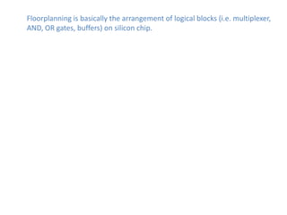
  • 1. Floorplanning is basically the arrangement of logical blocks (i.e. multiplexer, AND, OR gates, buffers) on silicon chip.
  • 2. Floorplanning is basically the arrangement of logical blocks (i.e. multiplexer, AND, OR gates, buffers) on silicon chip. It is attained by following steps: • Partition and synthesize larger designs into smaller modules consisting of IP’s and std cells
  • 3. Floorplanning is basically the arrangement of logical blocks (i.e. multiplexer, AND, OR gates, buffers) on silicon chip. It is attained by following steps: • Define width and Height of ‘core’ and ‘Die’ using the physical area of synthesized netlist, utilization factor and aspect ratio
  • 4. Floorplanning is basically the arrangement of logical blocks (i.e. multiplexer, AND, OR gates, buffers) on silicon chip. It is attained by following steps: • Define locations of pre-placed cells
  • 5. Floorplanning is basically the arrangement of logical blocks (i.e. multiplexer, AND, OR gates, buffers) on silicon chip. It is attained by following steps: • Place de-coupling capacitors surrounding pre-placed cells
  • 6. Floorplanning is basically the arrangement of logical blocks (i.e. multiplexer, AND, OR gates, buffers) on silicon chip. It is attained by following steps: • Power Planning
  • 7. Floorplanning is basically the arrangement of logical blocks (i.e. multiplexer, AND, OR gates, buffers) on silicon chip. It is attained by following steps: • IO Pin/Pad placement
  • 8. • We have defined the Width and Height of the core. • Also defined the locations of pre-placed cells. • We have encapsulated the Pre-placed Cells by Decoupling capacitor. • We will do the Power Planning for the Chip
  • 9. Power Planning Power Planning is to connect each cell in the design to the power source i.e. VDD and VSS. • If observed, while drawing any circuit on paper, we have only one 'vdd' at the top and one 'vss' at the bottom. • But on a chip, it becomes necessary to have a grid structure for power source, with more than one 'vdd' and 'vss‘. 3/2/2013 9
  • 10. We will convert the power lines into the Power Mesh.
  • 11. DECAP1 D Block a Block b 4 Pre-placed DECAP2 Cells Block c DECAP3 Die Core
  • 12. DECAP1 D Block a Block b 4 DECAP2 Block c DECAP3 Die Core
  • 13. DECAP1 D Block a Block b 4 DECAP2 Block c DECAP3 Die Vss Core Vdd
  • 14. DECAP1 D Block a Block b 4 DECAP2 Block c DECAP3 Die Vss Core Vdd
  • 15. DECAP1 D Block a Block b 4 DECAP2 Block c DECAP3 Die Vss Core Vdd
  • 16. DECAP1 D Block a Block b 4 DECAP2 Block c DECAP3 Die Vss Core Vdd
  • 17. DECAP1 D Block a Block b 4 DECAP2 Block c DECAP3 Die Vss Core Vdd Contact
  • 18. DECAP1 D Block a Block b 4 DECAP2 Block c DECAP3 Die Vss Core Vdd Contact
  • 19. DECAP1 D Block a Block b 4 DECAP2 Block c DECAP3 Die Vss Core Vdd Contact
  • 20. The Power mesh will look as below.
  • 22. DECAP1 D Block a Block b 4 DECAP2 Block c DECAP3 Die Vss Core Vdd Contact