

Recomendados
Más contenido relacionado
La actualidad más candente
La actualidad más candente (19)
Destacado
Similar a 312742 ds
Similar a 312742 ds (20)
Más de ____
Último
Último (20)
312742 ds
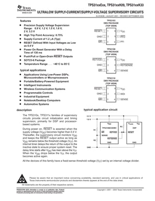
- 1. TPS31xxExx, TPS31xxH20, TPS31xxK33 ULTRALOW SUPPLYĆCURRENT/SUPPLYĆVOLTAGE SUPERVISORY CIRCUITS SLVS363B − AUGUST 2001 − REVISED SEPTEMBER 2004 www.ti.com 1 features D Precision Supply Voltage Supervision Range: 0.9 V, 1.2 V, 1.5 V, 1.6 V, 2 V, 3.3 V D High Trip Point Accuracy: 0.75% D Supply Current of 1.2 µA (Typ) D RESET Defined With Input Voltages as Low as 0.4 V D Power On Reset Generator With a Delay Time of 130 ms D Push/Pull or Open-Drain RESET Outputs D SOT23-6 Package D Temperature Range . . . −40°C to 85°C typical applications D Applications Using Low-Power DSPs, Microcontrollers or Microprocessors D Portable/Battery-Powered Equipment D Intelligent Instruments D Wireless Communication Systems D Programmable Controls D Industrial Equipment D Notebook/Desktop Computers D Automotive Systems description The TPS310x, TPS311x families of supervisory circuits provide circuit initialization and timing supervision, primarily for DSP and processor- based systems. During power on, RESET is asserted when the supply voltage (VDD) becomes higher than 0.4 V. Thereafter, the supervisory circuit monitors VDD and keeps the RESET output active as long as VDD remains below the threshold voltage (VIT). An internal timer delays the return of the output to the inactive state to ensure proper system reset. The delay time starts after VDD has risen above the VIT. When the VDD drops below the VIT, the output becomes active again. All the devices of this family have a fixed-sense threshold voltage (VIT) set by an internal voltage divider. Copyright 2001 − 2004 Texas Instruments IncorporatedPRODUCTION DATA information is current as of publication date. Products conform to specifications per the terms of Texas Instruments standard warranty. Production processing does not necessarily include testing of all parameters. Please be aware that an important notice concerning availability, standard warranty, and use in critical applications of Texas Instruments semiconductor products and disclaimers thereto appears at the end of this data sheet. All trademarks are the property of their respective owners. (TOP VIEW) RESET GND MR VDD PFI TPS3103 DBV PACKAGE PFO (TOP VIEW) RSTVDD GND MR VDD SENSE TPS3106 DBV PACKAGE RSTSENSE (TOP VIEW) RESET GND MR VDD SENSE TPS3110 DBV PACKAGE WDI TPS3106E33DBV VDD RSTVDD RSTSENSE GND SENSE R1 R2 GND Vcore VIO RESET R3 DSP 3.3 V 1.6 V GND typical application circuit 3 2 4 61 5 3 2 4 61 5 3 2 4 61 5 MR
- 2. TPS31xxExx, TPS31xxH20, TPS31xxK33 ULTRALOW SUPPLYĆCURRENT/SUPPLYĆVOLTAGE SUPERVISORY CIRCUITS SLVS363B − AUGUST 2001 − REVISED SEPTEMBER 2004 www.ti.com 2 description (continued) The TPS3103 and TPS3106 have an active-low, open drain RESET output. The TPS3110 has an active-low push/pull RESET. The product spectrum is designed for supply voltages of 0.9 V up to 3.3 V. The circuits are available in a 6-pin SOT-23 package. The TPS31xx family is characterized for operation over a temperature range of −40°C to 85°C. AVAILABLE OPTIONS DEVICE RESET OUTPUT RSTSENSE, RSTVDD OUTPUT SENSE INPUT WDI INPUT PFO OUTPUT TPS3103 n Open drain n Open drain TPS3106 n Open drain n TPS3110 n Push-pull n n PACKAGE INFORMATION TA DEVICE NAME THRESHOLD VOLTAGE, VIT MARKING TPS3103E12DBVR‡ TPS3103E12DBVT§ 1.142 V PFWI TPS3103E15DBVR‡ TPS3103E15DBVT§ 1.434 V PFXI TPS3103H20DBVR‡ TPS3103H20DBVT§ 1.84 V PFYI TPS3103K33DBVR‡ TPS3103K33DBVT§ 2.941 V PGRI TPS3106E09DBVR{‡ TPS3106E09DBVT§ 0.86 V PFZI −40°C to 85°C TPS3106E16DBVR‡ TPS3106E16DBVT§ 1.521 V PGSI−40 C to 85 C TPS3106K33DBVR‡ TPS3106K33DBVT§ 2.941 V PGBI TPS3110E09DBVR‡ TPS3110E09DBVT§ 0.86 V PGII TPS3110E12DBVR‡ TPS3110E12DBVT§ 1.142 V PGJI TPS3110E15DBVR‡ TPS3110E15DBVT§ 1.434 V PGKI TPS3110K33DBVR{‡ TPS3110K33DBVT§ 2.941 V PGLI † TPS3106E09 and TPS3110K33 will be available in August 2001; all other versions will be available in October 2001. ‡ The DBVR passive indicates tape and reel of 3000 parts. § The DBVT passive indicates tape and reel of 250 parts.
- 3. TPS31xxExx, TPS31xxH20, TPS31xxK33 ULTRALOW SUPPLYĆCURRENT/SUPPLYĆVOLTAGE SUPERVISORY CIRCUITS SLVS363B − AUGUST 2001 − REVISED SEPTEMBER 2004 www.ti.com 3 ordering information TPS31 03 E 15 DBV R Reel Package Nominal Supply Voltage Typical Reset Threshold Voltage Functionality Family DEVICE NAME NOMINAL SUPPLY VOLTAGE, VN(dc) DEVICE NAME TYPICAL RESET THRESHOLD VOLTAGE, VIT TPS310xx09DBV TPS311xx09DBV 0.9 V TPS310XEXXDBV TPS311XEXXDBV VN(dc) − 5% TPS310xx12DBV TPS311xx12DBV 1.2 V TPS310XHXXDBV VN(dc) − 8% TPS310xx15DBV TPS311xx15DBV 1.5 V TPS310XKXXDBV TPS311XKXXDBV VN(dc) − 11% TPS310xx16DBV 1.6 V TPS310xx20DBV 2 V TPS310xx33DBV- TPS311xx33DBV 3.3 V Function Tables TPS3110† MR V(SENSE) > 0.551 V VDD > VIT RESET L x x L H 0 0 L H 0 1 L H 1 0 L H 1 1 H † Function of watchdog-timer not shown x = Don’t care TPS3103 MR V(PFI) > 0.551 V VDD > VIT RESET PFO L 0 x L L L 1 x L H H 0 0 L L H 0 1 H L H 1 0 L H H 1 1 H H TPS3106 MR V(SENSE) > 0.551 V VDD > VIT RSTVDD RSTSENSE L x x L L H 0 0 L L H 0 1 H L H 1 0 L H H 1 1 H H
- 4. TPS31xxExx, TPS31xxH20, TPS31xxK33 ULTRALOW SUPPLYĆCURRENT/SUPPLYĆVOLTAGE SUPERVISORY CIRCUITS SLVS363B − AUGUST 2001 − REVISED SEPTEMBER 2004 www.ti.com 4 functional block diagram _ + _ + Reset Logic and Timer VIT− 0.551 V VDD MR PFI GND RESET PFO TPS3103 _ + _ + Reset Logic and Timer 0.551 V VDD MR SENSE GND RSTVDD Reset Logic and Timer RSTSENSE TPS3106 VIT−
- 5. TPS31xxExx, TPS31xxH20, TPS31xxK33 ULTRALOW SUPPLYĆCURRENT/SUPPLYĆVOLTAGE SUPERVISORY CIRCUITS SLVS363B − AUGUST 2001 − REVISED SEPTEMBER 2004 www.ti.com 5 functional block diagram (continued) _ + _ + Reset Logic and Timer 0.551 V VDD MR SENSE GND RESET Watchdog Logic and Control WDI TPS3110 VIT−
- 6. TPS31xxExx, TPS31xxH20, TPS31xxK33 ULTRALOW SUPPLYĆCURRENT/SUPPLYĆVOLTAGE SUPERVISORY CIRCUITS SLVS363B − AUGUST 2001 − REVISED SEPTEMBER 2004 www.ti.com 6 timing diagram td td td td td VDD VIT 0.4 V SENSE VIT−(S) = 0.551 V RESET Output Condition Undefined MR PFI VIT−(S) = 0.551 V Output Condition Undefined PFO t t t t t t t Output Condition Undefined Output Condition Undefined Figure 1. Timing Diagram for TPS3103
- 7. TPS31xxExx, TPS31xxH20, TPS31xxK33 ULTRALOW SUPPLYĆCURRENT/SUPPLYĆVOLTAGE SUPERVISORY CIRCUITS SLVS363B − AUGUST 2001 − REVISED SEPTEMBER 2004 www.ti.com 7 timing diagram VDD VIT 0.4 V t t t t t Output Condition Undefined Output Condition Undefined Output Condition Undefined Output Condition Undefined td td td td RSTVDD SENSE VIT−(S) = 0.551 V RSTSENSE MR Figure 2. Timing Diagram for TPS3106
- 8. TPS31xxExx, TPS31xxH20, TPS31xxK33 ULTRALOW SUPPLYĆCURRENT/SUPPLYĆVOLTAGE SUPERVISORY CIRCUITS SLVS363B − AUGUST 2001 − REVISED SEPTEMBER 2004 www.ti.com 8 timing diagram VDD VIT 0.4 V t t Output Condition Undefined Output Condition Undefined t td VIT−(S) = 0.551 V SENSE RESET WDI MR td td td td td t(tout) x = Don’t Care Figure 3. Timing Diagram for TPS3110
- 9. TPS31xxExx, TPS31xxH20, TPS31xxK33 ULTRALOW SUPPLYĆCURRENT/SUPPLYĆVOLTAGE SUPERVISORY CIRCUITS SLVS363B − AUGUST 2001 − REVISED SEPTEMBER 2004 www.ti.com 9 Terminal Functions TERMINAL I/O DESCRIPTION NAME PART NO. I/O DESCRIPTION GND ALL 2 GND MR ALL 3 I Manual-reset input. Pull low to force a reset. RESET remains low as long as MR is low and for the timeout period after MR goes high. Leave unconnected or connect to VDD when unused. PFI TPS3103 4 I Power-fail input compares to 0.551 V with no additional delay. Connect to VDD if not used. PFO TPS3103 5 O Power-fail output. Goes high when voltage at PFI rises above 0.551 V. RESET TPS3103 TPS3110 1 O Active-low reset output. Either push-pull or open-drain output stage RSTSENSE TPS3106 5 O Active-low reset output. Logic level at RSTSENSE only depends on the voltage at SENSE and the status of MR. RSTVDD TPS3106 1 O Active-low reset output. Logic level at RSTVDD only depends on the voltage at VDD and the status of MR. SENSE TPS3106 TPS3110 4 4 I A reset will be asserted if the voltage at SENSE is lower than 0.551 V. Connect to VDD if unused VDD ALL 6 Supply voltage. Powers the device and monitors its own voltageVDD ALL 6 Supply voltage. Powers the device and monitors its own voltage WDI TPS3110 5 I Watchdog timer input. If WDI remains high or low longer than the time-out period, then reset is triggered. The timer clears when reset is asserted or when WDI sees a rising edge or a falling edge. detailed description watchdog The TPS3110 device integrates a watchdog timer that must be periodically triggered by a positive or negative transition of WDI. When the supervising system fails to retrigger the watchdog circuit within the time-out interval, RESET becomes active for the time period (td). This event also reinitializes the watchdog timer. manual reset (MR) Many µC-based products require manual-reset capability, allowing an operator or logic circuitry to initiate a reset. Logic low at MR asserts reset. Reset remains asserted while MR is low and for a time period (td) after MR returns high. The input has an internal 100-kΩ pull-up resistor, so it can be left open if it is unused. Connect a normally open momentary switch from MR to GND to create a manual reset function. External debounce is not required. If MR is driven from long cables or if the device is used in noisy environments, connecting a 0.1-µF capacitor from MR to GND provides additional noise immunity. PFI, PFO The TPS3103 has an integrated power-fail (PFI) comparator with a separate open drain (PFO) output can be used for low-battery detection, power-fail warning, or for monitoring a power supply other than the main supply. An additional comparator is provided to monitor voltages other than the nominal supply voltage. The power-fail input (PFI) will be compared with an internal voltage reference of 0.551 V. If the input voltage falls below the power-fail threshold (VIT−(S)), the power-fail output (PFO) goes low. If it goes above 0.551 V plus approximately 15-mV hysteresis, the output returns to high. By connecting two external resistors, it is possible to supervise any voltage above 0.551 V. The sum of both resistors should be approximately 1 MΩ, to minimize power consumption and to assure that the current into the PFI pin can be neglected compared with the current through the resistor network. The tolerance of the external resistors should be not more than 1% to ensure minimal variation of sensed voltage. If the power-fail comparator is unused, connect PFI to GND and leave PFO unconnected. For proper operation of the PFI-comparator the supply voltage (VDD) must be higher than 0.8 V.
- 10. TPS31xxExx, TPS31xxH20, TPS31xxK33 ULTRALOW SUPPLYĆCURRENT/SUPPLYĆVOLTAGE SUPERVISORY CIRCUITS SLVS363B − AUGUST 2001 − REVISED SEPTEMBER 2004 www.ti.com 10 SENSE The voltage at the SENSE input is compared with a reference voltage of 0.551 V. If the voltage at SENSE falls below the sense-threshold (VIT−(S)), reset is asserted. On the TPS3106, a dedicated RSTSENSE output is available. On the TPS3110, the logic signal from SENSE is OR-wired with the logic signal from VDD or MR. An internal timer delays the return of the output to the inactive state, once the voltage at SENSE goes above 0.551 V plus about 15 mV of hysteresis. For proper operation of the SENSE-comparator, the supply voltage must be higher than 0.8 V. ABSOLUTE MAXIMUM RATINGS OVER OPERATING FREE-AIR TEMPERATURE (UNLESS OTHERWISE NOTED)(1) Supply voltage, VDD (2) 3.6 V. . . . . . . . . . . . . . . . . . . . . . . . . . . . . . . . . . . . . . . . . . . . . . . . . . . . . . . . . . . . . . . . . . . . All other pins (2) −0.3 V to 3.6 V. . . . . . . . . . . . . . . . . . . . . . . . . . . . . . . . . . . . . . . . . . . . . . . . . . . . . . . . . . . . . . . . . . Maximum low output current, IOL 5 mA. . . . . . . . . . . . . . . . . . . . . . . . . . . . . . . . . . . . . . . . . . . . . . . . . . . . . . . . . . . Maximum high output current, IOH −5 mA. . . . . . . . . . . . . . . . . . . . . . . . . . . . . . . . . . . . . . . . . . . . . . . . . . . . . . . . . Input clamp current, IIK (VI < 0 or VI > VDD) ±10 mA. . . . . . . . . . . . . . . . . . . . . . . . . . . . . . . . . . . . . . . . . . . . . . . . Output clamp current, IOK (VO < 0 or VO > VDD) ±10 mA. . . . . . . . . . . . . . . . . . . . . . . . . . . . . . . . . . . . . . . . . . . . Continuous total power dissipation See Dissipation Rating Table. . . . . . . . . . . . . . . . . . . . . . . . . . . . . . . . . . . . . Operating free-air temperature range, TA −40°C to 85°C. . . . . . . . . . . . . . . . . . . . . . . . . . . . . . . . . . . . . . . . . . . . Storage temperature range, Tstg −65°C to 150°C. . . . . . . . . . . . . . . . . . . . . . . . . . . . . . . . . . . . . . . . . . . . . . . . . . . Soldering temperature 260°C. . . . . . . . . . . . . . . . . . . . . . . . . . . . . . . . . . . . . . . . . . . . . . . . . . . . . . . . . . . . . . . . . . . . (1) Stresses beyond those listed under “absolute maximum ratings” may cause permanent damage to the device. These are stress ratings only, and functional operation of the device at these or any other conditions beyond those indicated under “recommended operating conditions” is not implied. Exposure to absolute-maximum-rated conditions for extended periods may affect device reliability. (2) All voltage values are with respect to GND. For reliable operation, the device must not be operated at 3.6 V for more than t=1000h continuously. DISSIPATION RATING TABLE PACKAGE TA ≤ 25°C POWER RATING DERATING FACTOR ABOVE TA = 25°C TA = 70°C POWER RATING TA = 85°C POWER RATING DBV 437 mW 3.5 mW/°C 280 mW 227 mW recommended operating conditions MIN MAX UNIT Supply voltage, VDD (1) 0.4 3.3 V Input voltage, VI 0 VDD + 0.3 V High-level input voltage, VIH at MR, WDI 0.7 × VDD V Low-level input voltage, VIL at MR, WDI 0.3 × VDD V Input transition rise and fall rate at ∆t/∆V at MR, WDI 100 ns/V Operating free-air temperature range, TA −40 85 °C (1) For proper operation of SENSE, PFI, and WDI functions: VDD ≥ 0.8 V
- 11. TPS31xxExx, TPS31xxH20, TPS31xxK33 ULTRALOW SUPPLYĆCURRENT/SUPPLYĆVOLTAGE SUPERVISORY CIRCUITS SLVS363B − AUGUST 2001 − REVISED SEPTEMBER 2004 www.ti.com 11 electrical characteristics over recommended operating conditions (unless otherwise noted) PARAMETERS TEST CONDITIONS MIN TYP MAX UNIT VDD = 3.3 V, IOH = −3 mA VDD = 1.8 V, IOH = −2 mA 0.8 VDD VOH High-level output voltage VDD = 1.5 V, IOH = −1 mA 0.8 × VDD VVOH High-level output voltage VDD = 0.9 V, IOH = −0.4 mA V VDD = 0.5 V, IOH = −5 µA 0.7 × VDD VDD = 3.3 V, IOL = 3 mA Low-level output VDD = 1.5 V, IOL = 2 mA 0.3 VOL Low-level output voltage VDD = 1.2 V, IOL = 1 mA 0.3 VVOL voltage VDD = 0.9 V, IOL = 500 µA V RESET only VDD = 0.4 V, IOL = 5 µA 0.1 TPS31xxE09 0.854 0.86 0.866 TPS31xxE12 1.133 1.142 1.151 VIT− Negative-going input (1) TPS31xxE15 TA = 25°C 1.423 1.434 1.445 VVIT− Negative-going input threshold voltage (1) TPS31xxE16 TA = 25°C 1.512 1.523 1.534 V threshold voltage TPS31xxH20 1.829 1.843 1.857 TPS31xxK33 2.919 2.941 2.963 VIT−(S) Negative-going input threshold voltage (1) SENSE, PFI VDD ≥ 0.8 V, TA = 25°C 0.542 0.551 0.559 V 0.8 V ≤ VIT < 1.5 V 20 Vhys Hysteresis at VDD input 1.6 V ≤ VIT < 2.4 V 30 mVVhys Hysteresis at VDD input 2.5 V ≤ VIT < 3.3 V 50 mV T(K) Temperature coefficient of VIT−, PFI, SENSE TA = −40°C to 85°C −0.012 −0.019 %/K Vhys Hysteresis at SENSE, PFI input VDD ≥ 0.8 V 15 mV MR MR = VDD, VDD = 3.3 V −25 25 IIH High-level input current SENSE, PFI, WDI SENSE, PFI, WDI = VDD, VDD = 3.3 V −25 25 nA IIL Low-level input current MR MR = 0 V, VDD = 3.3 V −47 −33 −25 µA IIL Low-level input current SENSE, PFI, WDI SENSE, PFI, WDI = 0 V, VDD = 3.3 V −25 25 nA IOH High-level output current at RESET (2) Open drain VDD = VIT + 0.2 V, VOH = 3.3 V 200 nA VDD > VIT (average current), VDD < 1.8 V 1.2 3 IDD Supply current VDD > VIT (average current), VDD > 1.8 V 2 4.5 µADD VDD < VIT, VDD < 1.8 V 22 VDD < VIT, VDD > 1.8 V 27 Internal pull-up resistor at MR 70 100 130 kΩ Ci Input capacitance at MR, SENSE, PFI, WDI VI = 0 V to VDD 1 pF (1) To ensure the best stability of the threshold voltage, a bypass capacitor (ceramic, 0.1 µF) should be placed close to the supply terminals. (2) Also refers to RSTVDD and RSTSENSE
- 12. TPS31xxExx, TPS31xxH20, TPS31xxK33 ULTRALOW SUPPLYĆCURRENT/SUPPLYĆVOLTAGE SUPERVISORY CIRCUITS SLVS363B − AUGUST 2001 − REVISED SEPTEMBER 2004 www.ti.com 12 TIMING REQUIREMENTS AT RL = 1 MΩ, CL = 50 PF, TA = −40°C TO 85°C PARAMETER TEST CONDITIONS MIN TYP MAX UNIT tt(out) Time-out period at WDI VDD ≥ 0.85 V 0.55 1.1 1.65 s at VDD VIH = 1.1 × VIT, VIL = 0.9 × VIT−, VIT− = 0.86 V 20 at MR VDD ≥ VIT + 0.2 V, VIL = 0.3 × VDD, VIH = 0.7 × VDD 0.1 tw Pulse width at SENSE VDD ≥ VIT, VIH = 1.1 × VIT−(S), VIL = 0.9 × VIT−(S) 20 µstw Pulse width at PFI VDD ≥ 0.85 V, VIH = 1.1 × VIT−(S),VIL = 0.9 × VIT−(S) 20 µs at WDI VDD ≥ VIT, VIL = 0.3 × VDD, VIH = 0.7 × VDD 0.3 SWITCHING CHARACTERISTICS AT RL = 1 MΩ, CL = 50 PF, TA = −40°C TO 85°C PARAMETER TEST CONDITIONS MIN TYP MAX UNIT td Delay time VDD ≥ 1.1 × VIT, MR = 0.7 × VDD, See timing diagram 65 130 195 ms tPHL Propagation delay time, high-to-low level output VDD to RESET or RSTVDD delay VIH = 1.1 × VIT, VIL = 0.9 × VIT 40 µs tPLH Propagation delay time, low-to-high level output VDD to RESET or RSTVDD delay VIH = 1.1 × VIT, VIL = 0.9 × VIT 40 µs tPHL Propagation delay time, high-to-low level output SENSE to RESET or RSTSENSE delay VDD ≥ 0.8 V, VIH = 1.1 × VIT, VIL = 0.9 × VIT 40 µs tPLH Propagation delay time, high-to-low level output SENSE to RESET or RSTSENSE delay VDD ≥ 0.8 V, VIH = 1.1 × VIT, VIL = 0.9 × VIT 40 µs tPHL Propagation delay time, high-to-low level output PFI to PFO delay VDD ≥ 0.8 V, VIH = 1.1 × VIT, VIL = 0.9 × VIT 40 µs tPLH Propagation delay time, low-to-high level output PFI to PFO delay VDD ≥ 0.8 V, VIH = 1.1 × VIT, VIL = 0.9 × VIT 300 µs tPHL Propagation delay time, low-to-high level output MR to RESET. RSTVDD, RSTSENSE delay VDD ≥ 1.1 × VIT, VIL = 0.3 × VDD, 1 5 s tPLH Propagation delay time, low-to-high level output MR to RESET. RSTVDD, RSTSENSE delay DD IT VIL = 0.3 × VDD, VIH = 0.7 × VDD 1 5 µs
- 13. TPS31xxExx, TPS31xxH20, TPS31xxK33 ULTRALOW SUPPLYĆCURRENT/SUPPLYĆVOLTAGE SUPERVISORY CIRCUITS SLVS363B − AUGUST 2001 − REVISED SEPTEMBER 2004 www.ti.com 13 TYPICAL CHARACTERISTICS Table of Graphs FIGURE Supply current vs Supply voltage at TA = −40°C, 0°C, 25°C, 85°C 4 VOL Low-level output voltage vs Low-level output current at TA = −40°C, 0°C, 25°C, 85°C at 0.9 V, 3.3 V 5, 6 VOH High-level output voltage vs High-level output current at TA = −40°C, 0°C, 25°C, 85°C at 0.9 V, 3.3 V 7, 8 tw Minimum pulse duration at VDD vs Threshold overdrive voltage 9 VIT Normalized threshold voltage vs Free-air temperature 10 Figure 4 0 2 4 6 8 10 12 14 16 18 20 0 0.5 1 1.5 2 2.5 3 TA = 85°C TA = 25°C TA = 0°C TA = −40°C DDISupplyCurrent−−Aµ VDD − Supply Voltage − V TPS3110E09 SUPPLY CURRENT vs SUPPLY VOLTAGE SENSE = VDD MR = Open RESET = Open WDI: Triggered Figure 5 0 0.05 0.10 0.15 0.20 0.25 0.30 0 0.2 0.4 0.6 0.8 1 1.2 1.4 1.6 1.8 2 TA = 25°C TA = 0°C TA = −40°C TA = 85°C −Low-LevelOutputVoltage−V TPS3110E09 LOW-LEVEL OUTPUT VOLTAGE vs LOW-LEVEL OUTPUT CURRENT VOL IOL − Low-Level Output Current − mA VDD = 0.9 V SENSE = GND MR = GND WDI = GND
- 14. TPS31xxExx, TPS31xxH20, TPS31xxK33 ULTRALOW SUPPLYĆCURRENT/SUPPLYĆVOLTAGE SUPERVISORY CIRCUITS SLVS363B − AUGUST 2001 − REVISED SEPTEMBER 2004 www.ti.com 14 Figure 6 0 0.1 0.2 0.3 0.4 0.5 0.6 0.7 0.8 0.9 1 0 2 4 6 8 10 12 14 16 18 20 TA = 25°C TA = 0°C TA = −40°C TA = 85°C VDD = 3.3 V SENSE = GND MR = GND WDI = GND TPS3110E09 LOW-LEVEL OUTPUT VOLTAGE vs LOW-LEVEL OUTPUT CURRENT −Low-LevelOutputVoltage−VVOL IOL − Low-Level Output Current − mA Figure 7 0.60 0.65 0.70 0.75 0.80 0.85 0.90 −0.5−0.4−0.3−0.2−0.10 TA = 25°C TA = 0°C TA = −40°C TA = 85°C VDD = 0.9 V SENSE = VDD MR = VDD WDI : Triggered TPS3110E09 HIGH-LEVEL OUTPUT VOLTAGE vs HIGH-LEVEL OUTPUT CURRENT IOH − High-Level Output Current − mA −High-LevelOutputVoltage−VVOH Figure 8 TA = −40°C 2 2.2 2.4 2.6 2.8 3 3.2 3.4 −25−20−15−10−50 TA =−40°C TA = 0°C TA = 25°C TA = 85°C VDD = 3.3 V SENSE = VDD MR = VDD WDI : Triggered TPS3110K33 HIGH-LEVEL OUTPUT VOLTAGE vs HIGH-LEVEL OUTPUT CURRENT −High-LeveloutputVoltage−VVOH IOH − Low-Level Output Current − mA Figure 9 0 5 10 15 20 25 30 35 40 45 50 0 0.05 0.1 0.15 0.2 0.25 0.3 0.35 0.4 0.45 0.5 −MinimumPulseDurationat MINIMUM PULSE DURATION AT VDD vs THRESHOLD OVERDRIVE VOLTAGE VDD − Threshold Overdrive Voltage − V VDD−sµtw VDD = 3.3 V VDD = 0.9 V MR : Open SENSE = VDD
- 15. TPS31xxExx, TPS31xxH20, TPS31xxK33 ULTRALOW SUPPLYĆCURRENT/SUPPLYĆVOLTAGE SUPERVISORY CIRCUITS SLVS363B − AUGUST 2001 − REVISED SEPTEMBER 2004 www.ti.com 15 −NormalizedThresholdVoltage−V NORMALIZED THRESHOLD VOLTAGE vs FREE-AIR TEMPERATURE 0.992 0.994 0.996 0.998 1 1.002 1.004 1.006 1.008 −50 0 50 100 VIT TA − Free-Air Temperature − °C Figure 10 APPLICATION INFORMATION TPS3110K33 GND SENSE GND R1 R2 DSP RESET GND WDI Px.y V (CORE_th) + 0.551 V R1 ) R2 R2 VDD RESET VCORE VIO 3.3 V 1.5 V MR Figure 11. TPS3110 in a DSP-System Monitoring Both Supply Voltages
- 16. TPS31xxExx, TPS31xxH20, TPS31xxK33 ULTRALOW SUPPLYĆCURRENT/SUPPLYĆVOLTAGE SUPERVISORY CIRCUITS SLVS363B − AUGUST 2001 − REVISED SEPTEMBER 2004 www.ti.com 16 APPLICATION INFORMATION TPS3103H20 PFI GND R1 R2 MSP430 RESET GND Analog Circuit Px.x Py.x V (neg_th) + 0.551 V * R2 R1 ǒV DD * 0.551 VǓ † Resistor may be integrated in µC † † RESET PFO VDD VDD Low Power µC 2 V −2 V MR Figure 12. TPS3103 Monitoring a Negative Voltage
- 17. TPS31xxExx, TPS31xxH20, TPS31xxK33 ULTRALOW SUPPLYĆCURRENT/SUPPLYĆVOLTAGE SUPERVISORY CIRCUITS SLVS363B − AUGUST 2001 − REVISED SEPTEMBER 2004 www.ti.com 17 APPLICATION INFORMATION The TPS310x family has a quiescent current in the 1-µA to 2-µA range. When RESET, triggered by the voltage monitored at VDD, is active, the quiescent current increases to about 20 µA (see electrical characteristics). In some applications it is necessary to minimize the quiescent current even during the reset period. This is especially true when the voltage of a battery is supervised and the RESET is used to shut down the system or for an early warning. In this case the reset condition will last for a longer period of time. Especially when the battery is discharged, the current drawn from the battery should almost be zero. For this kind of applications the TPS3103 or TPS3106 are a good fit. To minimize current consumption it must be assured to select a version where the threshold voltage is lower than the voltage monitored at VDD. The TPS3106 has two reset outputs. One output (RSTVDD) is triggered from the voltage monitored at VDD. The other output (RSTSENSE) is triggered from the voltage monitored at SENSE. In the application shown in Figure 13, the TPS3106E09 is used to monitor the input voltage of two NiCd or NiMH cells. The threshold voltage (V(th) = 0.86 V) was chosen as low as possible to ensure that the supply voltage is always higher than the threshold voltage at VDD. The voltage of the battery is monitored using the SENSE input. The voltage divider was calculated to assert a reset using the RSTSENSE output at 2 x 0.8 V = 1.6 V. R1 + R2 ǒVTRIP VIT(S) *1Ǔ Where: VTRIP is the voltage of the battery at which a reset is asserted VIT(S) is the threshold voltage at SENSE = 0.551 V. R1 was chosen for a resistor current in the 1-µA range. With VTRIP = 1.6 V: R1 ≈ 1.9 × R2 R1 = 820 k, R2 = 430 k TPS3106E09DBV SENSE GND R1 R2 VDD RSTVDD RSTSENSE R3 2 Cell NiMH Reset Output MR Figure 13. Battery Monitoring With 3-µA Supply Current for Device and Resistor Divider
- 19. IMPORTANT NOTICE Texas Instruments Incorporated and its subsidiaries (TI) reserve the right to make corrections, modifications, enhancements, improvements, and other changes to its products and services at any time and to discontinue any product or service without notice. Customers should obtain the latest relevant information before placing orders and should verify that such information is current and complete. All products are sold subject to TI’s terms and conditions of sale supplied at the time of order acknowledgment. TI warrants performance of its hardware products to the specifications applicable at the time of sale in accordance with TI’s standard warranty. Testing and other quality control techniques are used to the extent TI deems necessary to support this warranty. Except where mandated by government requirements, testing of all parameters of each product is not necessarily performed. TI assumes no liability for applications assistance or customer product design. Customers are responsible for their products and applications using TI components. To minimize the risks associated with customer products and applications, customers should provide adequate design and operating safeguards. TI does not warrant or represent that any license, either express or implied, is granted under any TI patent right, copyright, mask work right, or other TI intellectual property right relating to any combination, machine, or process in which TI products or services are used. Information published by TI regarding third-party products or services does not constitute a license from TI to use such products or services or a warranty or endorsement thereof. Use of such information may require a license from a third party under the patents or other intellectual property of the third party, or a license from TI under the patents or other intellectual property of TI. Reproduction of information in TI data books or data sheets is permissible only if reproduction is without alteration and is accompanied by all associated warranties, conditions, limitations, and notices. Reproduction of this information with alteration is an unfair and deceptive business practice. TI is not responsible or liable for such altered documentation. Resale of TI products or services with statements different from or beyond the parameters stated by TI for that product or service voids all express and any implied warranties for the associated TI product or service and is an unfair and deceptive business practice. TI is not responsible or liable for any such statements. Following are URLs where you can obtain information on other Texas Instruments products and application solutions: Products Applications Amplifiers amplifier.ti.com Audio www.ti.com/audio Data Converters dataconverter.ti.com Automotive www.ti.com/automotive DSP dsp.ti.com Broadband www.ti.com/broadband Interface interface.ti.com Digital Control www.ti.com/digitalcontrol Logic logic.ti.com Military www.ti.com/military Power Mgmt power.ti.com Optical Networking www.ti.com/opticalnetwork Microcontrollers microcontroller.ti.com Security www.ti.com/security Telephony www.ti.com/telephony Video & Imaging www.ti.com/video Wireless www.ti.com/wireless Mailing Address: Texas Instruments Post Office Box 655303 Dallas, Texas 75265 Copyright 2004, Texas Instruments Incorporated
- 20. This datasheet has been downloaded from: www.DatasheetCatalog.com Datasheets for electronic components.