W35124128
•
0 recomendaciones•415 vistas

International Journal of Engineering Research and Applications (IJERA) is an open access online peer reviewed international journal that publishes research and review articles in the fields of Computer Science, Neural Networks, Electrical Engineering, Software Engineering, Information Technology, Mechanical Engineering, Chemical Engineering, Plastic Engineering, Food Technology, Textile Engineering, Nano Technology & science, Power Electronics, Electronics & Communication Engineering, Computational mathematics, Image processing, Civil Engineering, Structural Engineering, Environmental Engineering, VLSI Testing & Low Power VLSI Design etc.

Recomendados
Más contenido relacionado
La actualidad más candente
La actualidad más candente (13)
Destacado
Destacado (20)
Similar a W35124128
Similar a W35124128 (20)
Último
Último (20)
W35124128
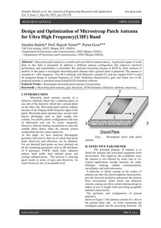
- 1. Jitendra Badole et al. Int. Journal of Engineering Research and Application ww.ijera.com Vol. 3, Issue 5, Sep-Oct 2013, pp.124-128 www.ijera.com 124 | P a g e Design and Optimization of Microstreap Patch Antenna for Ultra High Frequency(UHF) Band Jitendra Badole*, Prof. Rajesh Nema**, Puran Gour*** *(M Tech Scholar, NIIST, Bhopal, M.P., INDIA) *(Department Of Electronics and Communication, NIIST Bhopal, INDIA) ** (Department Of Electronics and Communication, NIIST Bhopal, INDIA) Abstract : Microstrip patch antenna is versatile and vast field of antenna theory. A particular aspect of work done in this field is presented. In addition a different antenna configuration that improves electrical performance and sustainability is described. We analyzed microstrip antenna in IE3D by finite moment of method. In this paper a rectangular microstrip patch antenna with a ground plane is proposed. The antenna is resonant at 1 GHz frequency. The FR-4 substrate with Dielectric constant 4.3 and loss tangent 0.019 is used for proposed design at resonant frequency of 1GHz. Radiation characteristics, gain and return loss of the proposed antenna is simulated using Zeland IE3D simulation software. General Terms :- Rectangular microstrip patch antenna, Ground plane Keywords :- Microstrip patch antenna, gain, directivity, IE3D Simulator, Dielectric substrate, return loss. I. INTRODUCTION Microstrip patch antenna consists of a dielectric substrate which has a radiating patch on one side of the dielectric which has a ground plane on the other side. Microstrip patch antenna radiates because of the fringing fields along the edges of the patch. Microstrip patch antennas have several well- known advantages such as light weight, low volume, low profile planar configurations and ease of fabrication and can be easily integrated. However, intricate feeding mechanisms to meet the suitable phase delays make the antenna system complicated and also cause signal loss. In this paper we have analyzed Rectangular geometry and tried to find out at which feed point better directivity and efficiency can be obtained. For our detected feed points we have checked out all the remaining parameters such as dB and phase of S parameter, VSWR, Smith chart, radiation pattern, band width, total radiated power and average radiated power. The structure is showing good results in terms of gain and directivity. Its return losses are also of acceptable level. Fig.1. Rectangular micro strip patch antenna II. EFFECTIVE PARAMETER The principal purpose of antenna is to shield the antenna and associated equipment from environment. This improves the availability since the antenna is not affected by wind, rain or ice. Typical applications include antennas for radar, telemetry, tracking, cellular communications, surveillance, and radio astronomy. A dielectric or ferrite coating on the surface of antenna can alter the electromagnetic characteristic, provide electrical insulation and protect the antenna from environment. Some ferrite and dielectric ceramic coating can allow certain antenna design to reduce in size or height while providing acceptable radiation characteristic. The geometry and configuration of praised antenna is shown in Figure 1.The antenna consists of a slot on the ground plane and via holes connecting the rectangular patch and the microstrip feed-line. All RESEARCH ARTICLE OPEN ACCESS
- 2. Jitendra Badole et al. Int. Journal of Engineering Research and Application ww.ijera.com Vol. 3, Issue 5, Sep-Oct 2013, pp.124-128 www.ijera.com 125 | P a g e of these are mounted on a square substrate of a thickness of 1.5 mm and a relative permittivity of 4.3 with length and width of 71.07568 mm and 92.144 mm respectively. The effective parameters which define the required geometries effective length and breadth of rectangular patch. Theoretical analysis and calculation of a single microstrip patch is calculated with following equations. The first step is to find the width of rectangular patch. Width of rectangular patch is given by: Where C is speed of light=3*10^11 mm, fo is resonant frequency=1Ghz & εr is Dielectric constant of the substrate=4.3 Effective dielectric constant is given by: Change in length is given by: Where, h is the height of the substrate. εeff, effective dielectric constant Effective length is given by: Where, εeff is the effective dielectric constant of the substrate. To measure for the fringing effects, the actual length of the patch also includes the correction factor due to fringing effect Actual length is given by: Taking FR-4 substrate with Dielectric constant εr 4.3 and loss tangent 0.019 is used for proposed design at resonant frequency (fo) of 1 GHz. the above parameters comes out to be W = 92.144 mm, εr eff = 4.4539, ΔL = 0.6941 mm, Leff = 71.07568 mm, L = 69.6874 mm. Ground patch of the geometry is design with the following equations: Length of ground patch, Lg = 6h+Leff Width of ground patch, Wg = 6h+W Lg = 80.07568 mm Wg= 101.144 mm Table 1. Antenna Design parameters: Antenna parameters Dimensions Resonant frequency fo 1 GHz Dielectric constant εr 4.3 Height of Substrate (h) 1.5 mm Width (W) 92.144 mm Length (L) 71.07568 mm Effective dielectric substrate εr eff 4.4539 Width of ground patch Wg 101.144 mm Length of ground patch Lg 80.7568 mm III.PROPOSED ANTENNA DESIGN Fig.2. Geometry of proposed single patch array Antenna IV .SIMULATED MICROSTRIP RECTANGULAR PATCH ANTENNA DESIGN AND RESULTS The proposed geometry of microstrip antenna designed with IE3D and simulation is performed . At the resonant frequency of 1GHz the design is simulated in the frequency range of 0 to 0.6GHz. The radiation pattern is bidirectional. The
- 3. Jitendra Badole et al. Int. Journal of Engineering Research and Application ww.ijera.com Vol. 3, Issue 5, Sep-Oct 2013, pp.124-128 www.ijera.com 126 | P a g e simulated results, return losses versus frequency for geometry shown in fig.4.We are getting better return loss at four different frequency are -25.88dB at .1224 GHz , -25.83dB at .2204 GHz,-20.56dB at .4653 GHz and -18.55dB at .551GHz and The frequency bands for these with return losses(below -10dB) of the proposed antenna are: a) 0.01GHz to 0.159 GHz b) 0.16GHz to 0.365 GHz c) 0.454GHz to 0.477 GHz d) 0.538GHz to 0.56 GHz The simulated return losses versus frequency graph shown in fig.4. The Impedance matching is shown in smith chart is shown in fig.6, its shows proper impedance matching, VSWR is near about 1 as shown on fig.3. (1) VSWR VS FREQUENCY VSWR IS effective and minimum between 0 to 0.6 GHz Fig.3. VSWR Vs Frequency (in GHz) For proposed design the value of VSWR is effective between 0GHz to 0.35GHz, for this value return loss is minimum. At 0.1224 GHz return loss is -25.88dB and VSWR is 1.107, which is minimum value. (2) RETURN LOSS VS FREQUENCY (IN GHz) At frequency of 0.1224 GHz the value of return loss is -25.88 dB Fig . 4. Retrun loss vs Frequency (in GHz) (3) S PARAMETER (magnitude in dB and phase) VS FREQUENCY (IN GHz) Fig.5.S Parameters Vs Frequency (in GHz) (4) SMITH CHART
- 4. Jitendra Badole et al. Int. Journal of Engineering Research and Application ww.ijera.com Vol. 3, Issue 5, Sep-Oct 2013, pp.124-128 www.ijera.com 127 | P a g e Fig.6. Smith Chart (5) DIRECTIVITY VS FREQUENCY (IN GHz) Fig.7. Directivity Vs Frequency (in GHz) (6) RADIATION PATTERN: Fig.8. Radiation Pattern (7) 3D PATTERN OF THE ANTENNA Fig.9. 3D Pattern V.SIMULATION TABLE Sn. Frequency (in GHz) Return loss (in dB) VSWR 1 0.01224 -10.68 1.826 2 0.02449 -14.44 1.468 3 0.03673 -15.27 1.417 4 0.04898 -11.79 1.693 5 0.06122 -13.69 1.522 6 0.07347 -12.13 1.657 7 0.8571 -11.76 1.697 8 0.09796 -12.92 1.584 9 0.1102 -15.25 1.418 10 0.1224 -25.88 1.107 11 0.1347 -16.17 1.368 12 0.1469 -10.69 1.825
- 5. Jitendra Badole et al. Int. Journal of Engineering Research and Application ww.ijera.com Vol. 3, Issue 5, Sep-Oct 2013, pp.124-128 www.ijera.com 128 | P a g e 13 0.1592 -9.827 1.952 14 0.1714 -13.27 1.554 15 0.1837 -20.88 1.199 16 0.1959 -17.32 1.315 17 0.2082 -16.69 1.343 18 0.2204 -25.83 1.108 19 0.2327 -20.23 1.26 20 0.2449 -17.5 1.308 21 0.2571 -16.51 1.352 22 0.2694 -18.28 1.278 23 0.2816 -17.34 1.314 24 0.2939 -12.06 1.665 25 0.3061 -10.56 1.842 26 0.3184 -13.04 1.573 27 0.3306 -16.8 1.338 28 0.3429 -12.97 1.58 29 0.3551 -11.1 1.772 30 0.3673 -9.278 2.047 31 0.3796 -5.927 3.044 32 0.3918 -5.169 3.459 33 0.4041 -5.697 3.158 34 0.4163 -5.687 3.163 35 0.4286 -4.965 3.594 36 0.4408 -5.509 3.258 37 0.4531 -9.683 1.976 38 0.4653 -20.56 1.207 39 0.4776 -9.479 3.011 40 0.4898 -5.998 3.01 41 0.502 -4.529 3.922 42 0.5143 -4.514 3.934 43 0.5265 -5.844 3.084 44 0.5388 -10.5 1.852 45 0.551 -18.155 1.268 46 0.5633 -8.063 2.307 47 0.5755 -4.177 4.239 48 0.5878 -2.923 6 49 0.6 -2.926 5.993 CONCLUTION A novel antenna with via holes at UHF is illustrated in this paper. It consists of a ground plane, a rectangular microstrip patch slot and a via hole connecting the rectangular patch and the microstrip feed-line. The better return losses are due to the slots cut in the rectangular patch and by connecting via hole. The antenna is resonant at 1GHz frequency and simulated up to 0.6GHz. The return loss obtained is -25.88 dBi at .1224 GHz VSWR is 1.107, which is minimum value. . The return losses at four frequency bands are -25.88dB at .1224 GHz , -25.83dB at .2204 GHz,-20.56dB at .4653 GHz and -18.55dB at 0.551GHz and The frequency bands for these with return losses(below -10dB) of the proposed antenna are: a) 0.01GHz to 0.159 GHz b) 0.16GHz to 0.365 GHz c) 0.454GHz to 0.477 GHz d) 0.538GHz to 0.56 GHz This antenna is very easy to fabricate and implement in any circuit and also of low cost as this structure is not complicated. The antenna is successfully designed, constructed, and measured. ACKNOWLEDGEMENT The author of this paper are thankful for the director of the NRI Institute of Information Science and Technology, Bhopal for making the simulation tool IE3D available for designing and simulation of the proposed antenna. The author is also thankful for Mr. Rajesh Nema H.O.D. of Electronics & Communication,Mr. Puran Gour(Assoc. Prof. of EC Dept.) and Mr. Rajeev Thakur(Assoc. Prof. of EC Dept.) of the same institute who encouraged me tremendously during the designing process and also during the literature review. REFERENCES [1] Jun Zhang, Yunliang Long, Senior Member, IEEE “A Dual-layer Broadband Compact UHF RFID Tag Antenna for Platform Tolerant Application “2013 [2] Balanis C.A(1982) Handbook of Microstrip Antennas. John Wiley and Sons New York [3] New Multiband E-Shape Microstrip Patch Antenna On RT DUROID 5880 Substrate and RO4003 Substrate for Pervasive Wireless Communication. Dr. Anubhuti Khare, Rajesh Nema and Puran Gour [4] Bojana Zivanovic, Thomas M. Weller , and Carlos Coatas “Series-Fed Microstrip Antenna Array and Their Applications to Omni-Directional Antenna ”, IEEE Trans. AntennaPropag., Vol.60,No.10. pp.4954- 4959,October 2012 [5] Experimental Investigation of an Equilateral Triangular Microstrip Antenna with a Dielectric Radome. Manotosh Biswas and Debatosh Guha, Institute of Radio Physics and Electronics, University of Calcutta, Kolkata (India). International Conference on Microwave – 08. [6] Qing-Xin Chu, Member, IEEE, and Ying- Ying Yang, “A Compact Ultra wideband Antenna With 3.4/5.5 GHz Dual Band- Notched Characteristics”, IEEE Transactions on Antennas And Propagation, Vol. 56, No. 12, December 2008. [7] G. Kumar and K.P. Ray, ” Broadband Microstrip Antennas”, Artech House, 2003.