DC MOTOR CONTROL MODULE
•Descargar como DOCX, PDF•
1 recomendación•416 vistas

This document describes an Android-based DC motor control module that uses an ATmega8 microcontroller and MOSFETs. The module features include high performance, efficiency, reliability, and precise speed control of DC motors using pulse-width modulation (PWM) signals. An H-bridge circuit configuration with MOSFETs is used to control the direction of the DC motor. The document provides details on the components used, including descriptions of the ATmega8 microcontroller, MOSFETs, and H-bridge circuit.

Recomendados
Más contenido relacionado
La actualidad más candente
La actualidad más candente (20)
Destacado
Destacado (20)
Similar a DC MOTOR CONTROL MODULE
Similar a DC MOTOR CONTROL MODULE (20)
DC MOTOR CONTROL MODULE
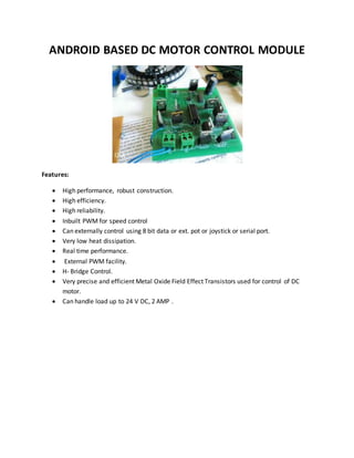
- 1. ANDROID BASED DC MOTOR CONTROL MODULE Features: High performance, robust construction. High efficiency. High reliability. Inbuilt PWM for speed control Can externally control using 8 bit data or ext. pot or joystick or serial port. Very low heat dissipation. Real time performance. External PWM facility. H- Bridge Control. Very precise and efficient Metal Oxide Field Effect Transistors used for control of DC motor. Can handle load up to 24 V DC, 2 AMP .
- 2. Introduction: It gives us great pleasure in presenting DC MOTOR CONTROL MODULE for electronics developer, robotics engineers, engineering students and Industrial engineers etc. Now a day’s electronics are widely used in our daily life, like coffee maker, mobile phone, oven, laptop etc. Our lifestyle is totally depends on electronics , we wake in morning through alarm on mobile phone, we make coffee on coffee maker, we use oven , greaser, electric iron, induction cooker, washing machine, computer, calculator and so many other things in our daily life. So it’s time to take a step towards electronics to make better life style. Electronics also used in Industrial control system and automation. Electronics makes things easier, chipper and better. Here we have introduced a Module for Industrial, robotics and for other electronics projects. DC motor is widely used in Robotics, some Industrial applications and in engineering students Projects. To use it in any application we need precise control. By using this Module we can control DC motor very precisely, accurately and efficiently in any application. DC MOTOR CONTROL: For permanent magnet DC motor, by varying armature voltage we can control its torque. And by controlling the torque means we can control speed of PMDC Motor. For Direction control of motor we just have to interchange the supply terminals. So these are the steps to control DC motor. In our module we have using PWM for speed control and H-bridge for direction control of DC Motor. By this means our module will control PMDC motor very precisely, accurately and efficiently. Here we have also use microcontroller to build PWM and to drive H-bridge. Our microcontroller has inbuilt PWM and ADC for controlling of the speed of motor. Here we also can control of PMDC Motor through external means like Joystick, serial port (Wi-Fi, Bluetooth, PC etc.) and 8 bit data.
- 3. MOSFET: MOSFET stands for Metal Oxide Semiconductor Field Effect Transistor. It has two types viz., depletion type MOSFET and Enhancement type MOSFET. The MOSFET transistor has become one of the most important devices used in the design and construction of integrated circuits for digital computers. As noted above, there are differences in the characteristics and operation of each type of MOSFET. In below we will examine the enhancement-type MOSFET. Fig. 1. The basic construction of the n-channel enhancement-type MOSFET is shown in fig. 1. A slab of p-type material is formed from a silicon base and is referred to as a substrate. In Enhancement-type MOSFET forth lead is made available for external control of its potential level. The source and drain terminals are again connected through metallic contacts to n-doped regions. The SiO2 layer is present to isolate the gate metallic platform from the region between the drain and source, but it is simply separated from a section of the p-type material.
- 4. Fig.2. If Vgs is set at 0V and a voltage applied between the drain and source of the device of fig. 2, the absence of an n-channel will result in a current of effectively zero amperes. It is not sufficient to have a large accumulation of carriers (electrons) at the drain and source if a path fails to exist between the two. With Vds some positive voltage, Vgs at 0V, and terminal SS directly connected to the source, there are in fact two reverse-biased p-n junctions between the n-doped regions and the p-substrate to oppose any significant flow between drain and source.
- 5. Fig.3 In fig.3 both Vds and Vgs have been set at some positive voltage greater than 0V, establishing the drain and gate at a positive potential with respect to the source. The positive potential at the gate will pressure the holes in the p-substrate, as shown in fig. The result is a depletion region near the SiO2 insulating layer void of holes. However, the electrons in the p- substrate will be attracted to the positive gate terminal. As Vgs increases in magnitude, the concentration of electrons near the SiO2 surface increases until eventually the induced n-type region can support a measurable flow between drain and source. The level of Vgs that results in the significant increase in drain current is called threshold voltage and is given the symbol Vt. On specification sheets it is referred to as Vgst, although Vt is less unwieldy and will be used in
- 6. the analysis to follow. Since the channel is nonexistent with Vgs=0V and enhanced by the application of a positive gate-to-source voltage, this type of MOSFET is called an enhancement- type MOSFET. Fig. 4 shows the characteristics of Enhancement-type MOSFET. Fig.4.
- 7. H-BRIDGE Fig. 5 shows the circuit diagram of H-Bridge based on MOSFET. Here we have used two p-channel MOSFET and two n-channel MOSFET. All are Enhancement-type MOSFETs. As shown in fig. 5, pull up resistors are used to provide positive voltage to the gate. The gate terminal should not be left floating, it is dangerous for the device. Fig.5. When we provide negative voltage to the both the gate terminals, the both p-channel MOSFET will go under conduction mode and similarly both n-channel MOSFET will go under blocking mode. So the both the terminals of the motor will purposively getting positive voltage. Motor will not run.
- 8. When we apply positive voltage to the left gate terminal and same time we apply negative voltage to the right gate terminal, the left p-channel MOSFET will go under blocking mode and left n-channel MOSFET will go under conduction mode. Similarly, right p-channel MOSFET will go under conduction mode and right n-channel MOSFET will go under blocking mode. Motor will run in Reverse Direction. When we apply positive voltage to the right gate terminal and same time we apply negative voltage to the left gate terminal, the right p-channel MOSFET will go under blocking mode and right n-channel MOSFET will go under conduction mode. Similarly, left p-channel MOSFET will go under conduction mode and left n-channel MOSFET will go under blocking mode. Motor will run in Forward Direction. When we provide positive voltage to the both the gate terminals, the both n-channel MOSFET will go under conduction mode and similarly both p-channel MOSFET will go under blocking mode. So the both the terminals of the motor will purposively getting negative voltage. Motor will not run. So, this H-Bridge will work efficiently for controlling the direction of the DC Motor. We can also control the speed of the motor by applying the PWM signals to the both Gate terminals. But in our case we are using another p-channel MOSFET for controlling the speed of the DC Motor. The n-channel MOSFET can also used for the same. Refer circuit diagram of fig. 6. By applying the PWM signal to the gate terminal of the MOSFET we can easily control the speed of the MOSFET. PWM is the best efficient method to use for various applications viz. speed control of DC motor/AC motor, firing angle control of TRIAC, IGBT and SCR etc. So, basically it is most popular method for DC Motor Speed control.
- 9. AT mega 8 Microcontroller: Features: • High-performance, Low-power Atmel®AVR® 8-bit Microcontroller • Advanced RISC Architecture – 130 Powerful Instructions – Most Single-clock Cycle Execution – 32 × 8 General Purpose Working Registers – Fully Static Operation – Up to 16MIPS Throughput at 16MHz – On-chip 2-cycle Multiplier • High Endurance Non-volatile Memory segments – 8Kbytes of In-System Self-programmable Flash program memory – 512Bytes EEPROM – 1Kbyte Internal SRAM – Write/Erase Cycles: 10,000 Flash/100,000 EEPROM – Data retention: 20 years at 85°C/100 years at 25°C – Optional Boot Code Section with Independent Lock Bits In-System Programming by On-chip Boot Program True Read-While-Write Operation – Programming Lock for Software Security • Peripheral Features – Two 8-bit Timer/Counters with Separate Prescaler, one Compare Mode – One 16-bit Timer/Counter with Separate Prescaler, Compare Mode, and Capture Mode – Real Time Counter with Separate Oscillator – Three PWM Channels – 8-channel ADC in TQFP and QFN/MLF package Eight Channels 10-bit Accuracy – 6-channel ADC in PDIP package Six Channels 10-bit Accuracy – Byte-oriented Two-wire Serial Interface – Programmable Serial USART – Master/Slave SPI Serial Interface – Programmable Watchdog Timer with Separate On-chip Oscillator – On-chip Analog Comparator • Special Microcontroller Features – Power-on Reset and Programmable Brown-out Detection – Internal Calibrated RC Oscillator – External and Internal Interrupt Sources – Five Sleep Modes: Idle, ADC Noise Reduction, Power-save, Power-down, and Standby • I/O and Packages – 23 Programmable I/O Lines – 28-lead PDIP, 32-lead TQFP, and 32-pad QFN/MLF
- 10. • Operating Voltages – 2.7V - 5.5V (ATmega8L) – 4.5V - 5.5V (ATmega8) • Speed Grades – 0 - 8MHz (ATmega8L) – 0 - 16MHz (ATmega8) • Power Consumption at 4 MHz, 3V, 25°C – Active: 3.6mA – Idle Mode: 1.0mA – Power-down Mode: 0.5μA
- 11. PIN DIAGRAM:
- 13. REFERENCES: [1] 4QD. Ncc70 reference manual.Technical report.URL: http://www.4qd.co.uk/. [2] Intersil.Hip4081a data sheet.Technical report.URL: http://www.intersil.com/. [3] International Rectifier.Powermosfetapplicationnotesanddatasheets.Technical report.URL: http://www.irf.com/. [4] Al Williams (2002). Microcontroller projects using the Basic Stamp (2nd ed.). Focal Press. p. 344. ISBN 978- 1-57820-101-3. [5] "The Half-bridge Circuit Revealed" Tom Ribarich (2012) [6] Atmega 8 Datasheet [7] www.netrino.com – Introduction to Pulse Width Modulation (PWM) [8] http://ww1.microchip.com/downloads/en/DeviceDoc/70187E.pdf [9] https://en.wikipedia.org/wiki/MOSFET