SlideShare una empresa de Scribd logo
1 de 5
Technical Article
MS-2446
.
www.analog.com
Page 1 of 5 ©2013 Analog Devices, Inc. All rights reserved.
The ABCs of Interleaved ADCs
by Jonathan Harris, Applications Engineer, Analog
Devices, Inc.
INTRODUCTION
Across many segments of the market today, interleaving
ADCs offers several advantages in many applications. In
communications infrastructure there is constantly a push for
higher sample rate ADCs to allow for multiband, multicarrier
radios, in addition to wider bandwidth requirements for
linearization techniques like DPD (digital predistortion). In
military and aerospace, higher sample rate ADCs allow for
multipurpose systems that can be used for communications,
electronic surveillance, and radar just to name a few. In yet
another segment, industrial instrumentation, the need is
always increasing for higher sample rate ADCs so that higher
speed signals can be measured adequately and accurately.
It is first important to understand exactly what interleaving
ADCs is about. To understand interleaving, it is good to look
at what is actually happening and how it is being implemented.
With a basic understanding, the benefits of interleaving can
then be discussed. Of course, as many know, there is no such
thing as a free lunch, so the challenges of interleaving need
to be evaluated and assessed.
ABOUT INTERLEAVING
When ADCs are interleaved, two or more ADCs with a
defined clocking relationship are used to simultaneously
sample an input signal and produce a combined output
signal that results in a sampling bandwidth at some multiple
of the individual ADCs. Utilizing m number of ADCs allows
for the effective sample rate to be increased by a factor of m.
For the sake of simplicity and ease of understanding, we’ll
focus on the case of two ADCs. In this case, if two ADCs
with each having a sample rate of fS are interleaved, the
resultant sample rate is simply 2fS. These two ADCs must
have a clock phase relationship for the interleaving to work
properly. The clock phase relationship is governed by
Equation 1, where n is the specific ADC and m is the total
number of ADCs.
∅ 𝑛 = 2𝜋 �
𝑛−1
𝑚
� (1)
As an example, two ADCs each, with a sample rate of
100 MSPS, are interleaved to achieve a sample rate of
200 MSPS. In this case, Equation 1 can be used to derive the
clock phase relationship of the two ADCs and is given by
Equation 2 and Equation 3.
∅1 = 2𝜋 �
1−1
2
� = 0 𝑟𝑎𝑑𝑖𝑎𝑛𝑠 = 0 𝑜
(2)
∅2 = 2𝜋 �
2−1
2
� = 𝜋 𝑟𝑎𝑑𝑖𝑎𝑛𝑠 = 180 𝑜
(3)
Now that the clock phase relationship is known, the
construction of samples can be examined. Figure 1 gives a
visual representation of the clock phase relationship and the
sample construction of two 100 MSPS interleaved ADCs.
Notice the 180° clock phase relationship and how the samples
are interleaved. The input waveform is alternatively sampled
by the two ADCs. In this case, the interleaving is implemented
by using a 200 MHz clock input that is divided by a factor of
two and the required phases of the clock to each ADC.
Figure 1. Two Interleaved 100 MSPS ADCs—Basic Diagram
Another representation of this concept is illustrated in
Figure 2. By interleaving these two 100 MSPS ADCs, the
sample rate is increased to 200 MSPS. This extends each
Nyquist zone from 50 MHz to 100 MHz, doubling the
available bandwidth in which to operate. The increased
operational bandwidth brings many advantages to applications
across many market segments. Radio systems can increase
the number of supported bands; radar systems can improve
spatial resolution, and measurement equipment can achieve
greater analog input bandwidth.
Figure 2. Two Interleaved 100 MSPS ADCs—Clocking and Samples
MS-2446 Technical Article
Page 2 of 5
BENEFITS OF INTERLEAVING
The benefits of interleaving span across multiple segments of
the market. The most desired benefit of interleaving is the
increased bandwidth made possible by the wider Nyquist
zone of the interleaved ADCs. Once again, taking the
example of two 100 MSPS ADCs interleaved to create a
sample rate of 200 MSPS, Figure 3 gives a representation of
the much wider bandwidth allowed by interleaving the two
ADCs. This creates advantages for many different applications.
As cellular standards increase channel bandwidth and the
number of operating bands, there are increased demands on
the available bandwidth in the ADC. In addition, in military
applications, the requirements for better spatial recognition,
as well as increased channel bandwidths in backend com-
munications require higher bandwidths from the ADC. Due
to the increased demands for bandwidth in these areas, there
is a need created to measure these signals accurately. Therefore,
measurement equipment has increased needs for higher
bandwidths in order to properly acquire and measure these
signals that have higher bandwidth. The system requirements
in many designs inherently stay ahead of commercial ADC
technology. Interleaving allows for some of this gap to be closed.
Figure 3. Two Interleaved ADCs—Nyquist Zone
The increased sample rate provides more bandwidth for
these applications but also allows for easier frequency
planning and reduction in the complexity and cost of the
anti-aliasing filter that is typically used at the ADC inputs.
With all these great benefits, one has to wonder what the
price is to pay. As with most things, there is no such thing as
a free lunch. Interleaved ADCs offer increased bandwidth
and other nice benefits, but there are some challenges that
arise when dealing with interleaved ADCs.
CHALLENGES WITH INTERLEAVING
There are some challenges and things to look out for when
interleaving ADCs. There are spurs that appear in the output
spectrum that result from the imperfections associated with
interleaving ADCs. These imperfections are basically
mismatches between the two ADCs that are being
interleaved. There are four basic mismatches that result in
spurs in the output spectrum. These are offset mismatch,
gain mismatch, timing mismatch, and bandwidth mismatch.
The easiest of these to understand is probably the offset
mismatch between the two ADCs. Each ADC will have an
associated dc offset value. When the two ADCs are interleaved
and samples are acquired alternatively back and forth between
the two ADCs, the dc offset of each successive sample is
changing. Figure 4 gives an example of how each ADC has
its own dc offset and how the interleaved output will effectively
switch back and forth between these two dc offset values.
The output switches between these offset values at a rate
of fS/2 which will result in a spur in the output spectrum
located at fS/2. Since the mismatch itself does not have a
frequency component and is only at dc, the frequency of the
spur that appears in the output spectrum only depends on
the sampling frequency and will always appear at a frequency
of fS/2. The magnitude of the spur is dependent upon the
magnitude of the offset mismatch between the ADCs. The
greater the mismatch, the larger the spur will be. In order to
minimize the spur caused by the offset mismatch, it is not
necessary to completely null the dc offset in each ADC.
Doing this would filter out any DC content in the signal and
would not work for systems using a ZIF (zero IF) architecture
where the signal content is real and complex and includes
data at DC. Instead, a more appropriate technique would be
to match the offset of one of the ADCs to the other ADC.
The offset of one ADC is chosen as the reference, and the
offset of the other ADC is set to match that value as closely
as possible. The better matched the offset values are, the
lower the resulting spur is at fS/2.
The second mismatch to look at when interleaving is
the gain mismatch between the ADCs. Figure 5 gives a
representation of the gain mismatch between two interleaved
converters. In this case, there is a frequency component to
the mismatch. In order to observe this mismatch, there has
to be a signal applied to the ADCs. In the case of the offset
mismatch, no signal is necessary to see the inherent dc offset
of the two ADCs. In the case of the gain mismatch, there is
no way to see the gain mismatch unless a signal is present
and the gain mismatch can be measured. The gain mismatch
will result in a spur in the output spectrum that is related to
the input frequency, as well as the sampling rate, and will
appear at fS/2 ± fIN. In order to minimize the spur caused by
Technical Article MS-2446
Page 3 of 5
the gain mismatch, a similar strategy as what is used for the
offset mismatch is employed. The gain of one of the ADCs is
chosen as the reference, and the gain of the other ADC is set
to match that gain value as closely as possible. The better the
gain values of each ADC are matched to each other, the less
the resulting spur will be in the output spectrum.
Next, we must examine the timing mismatch between the
two ADCs. The timing mismatch has two components,
group delay in the analog section of the ADC and clock
skew. The analog circuitry within the ADC has an associated
group delay and the value can be different between the two
ADCs. In addition, there is clock skew that has an aperture
uncertainty component in each of the ADCs and has a
component related to the accuracy of the clock phases
that are input to each converter. Figure 6 gives a visual
representation of the mechanism and effects of the timing
mismatches in the ADCs. Similar to the gain mismatch spur,
the timing mismatch spur is also a function of the input
frequency and the sample rate and appears at fS/2 ± fIN.
In order to minimize the resulting spur, the group delay
through the analog section of each converter needs to be
properly matched with good circuit design techniques. In
addition, the clock path designs need to be closely matched
to minimize aperture uncertainty differences. And lastly, the
clock phase relationships need to be precisely controlled
such that the two input clocks are as close to 180° apart as
possible. As with the other mismatches, the goal is to
attempt to minimize the mechanisms that cause the timing
mismatch.
The last mismatch to look at is probably the most difficult to
comprehend and handle; it is the bandwidth mismatch. As
shown in Figure 7, the bandwidth mismatch has a gain and a
phase/frequency component. This makes bandwidth mismatch
more difficult because it contains components from two of
the other mismatch parameters. In the bandwidth mismatch,
however, we see different gain values at different frequencies.
In addition, the bandwidth has a timing component which
causes signals at different frequencies to have different
delays through each converter. The best way to minimize
the bandwidth mismatch is to have very good circuit design
and layout practices that work to minimize the bandwidth
mismatches between the ADCs. The better matched each
ADC is, the less the resulting spur will be. Just as the gain
and timing mismatches caused spurs in the output spectrum
at fS/2 ± fIN, the bandwidth mismatch also results in a spur at
the same frequency.
Figure 4. Offset Mismatch
Figure 5. Gain Mismatch
MS-2446 Technical Article
Page 4 of 5
Figure 6. Timing Mismatch
Figure 7. Bandwidth Mismatch
Now that we’ve discussed four different mismatches that
cause issues when interleaving ADCs, it is apparent that a
commonality has emerged. Three of the four mismatches
produce a spur in the output spectrum at fS/2 ± fIN. The
offset mismatch spur can be easily identified since it alone
resides at fS/2 and can be compensated fairly easily. The gain,
timing, and bandwidth mismatches all produce a spur at
fS/2 ± fIN in the output spectrum so the question is how to
identify the contribution of each. Figure 8 gives a quick
visual guide to the process of identifying the sources of the
spurs from the different mismatches of interleaved ADCs.
Figure 8. Interrelated Nature of Interleaving Mismatches
If looking purely at gain mismatch alone, it is a low
frequency, or dc, type of mismatch. The gain component
of the bandwidth mismatch can be separated from the gain
mismatch by performing a gain measurement at low
frequency near dc and then performing gain measurements
at higher frequencies. The gain mismatch is not a function
of frequency like the gain component of the bandwidth
mismatch. A similar approach is used for the timing mismatch.
A measurement is performed at low frequency near dc and
then subsequent measurements are performed at higher
frequencies to separate the timing component of bandwidth
mismatch from the timing mismatch.
CONCLUSION
The newest communication system designs, cutting edge
radar technologies, and ultrahigh bandwidth measurement
equipment seem to constantly outpace the available ADC
technology. These requirements push both users and
manufacturers of ADCs to develop methods to keep pace
with these demands. Interleaving ADCs allows for greater
bandwidths to be achieved at a faster pace than the traditional
path of increasing the conversion rate of a typical ADC. By
taking two or more ADCs and interleaving them together,
the available bandwidth is increased, and system design
requirements can be met at a faster pace. Interleaving ADCs
does not come for free, however, and mismatches between
the ADCs cannot be ignored. Even though the mismatches
do exist, knowing about them and how to appropriately deal
with them can enable designers to use these interleaved ADCs
more intelligently and meet the ever increasing demands of
their latest system designs.
Technical Article MS-2446
Page 5 of 5
REFERENCES
Had, Jim, Mark Looney, and Rob Reeder. “Pushing the State
of the Art with Mulitchannel A/D Converters.” Analog
Dialogue. Vol. 39, No. 5, May 2005.
RESOURCES
Share this article on
One Technology Way • P.O. Box 9106 • Norwood, MA 02062-9106, U.S.A.
Tel: 781.329.4700 • Fax: 781.461.3113 • www.analog.com
Trademarks and registered trademarks are the property of
their respective owners. TA11329-0-1/13
www.analog.com
©2013 Analog Devices, Inc. All rights reserved.

Más contenido relacionado

La actualidad más candente

Performance analysis of radar based on ds bpsk modulation technique
Performance analysis of radar based on ds bpsk modulation techniquePerformance analysis of radar based on ds bpsk modulation technique
Performance analysis of radar based on ds bpsk modulation techniqueIAEME Publication
 
Ch5 Data communication and networking by neha g. kurale
Ch5 Data communication and networking by neha g. kuraleCh5 Data communication and networking by neha g. kurale
Ch5 Data communication and networking by neha g. kuraleNeha Kurale
 
SpyropulosPaper
SpyropulosPaperSpyropulosPaper
SpyropulosPaperchuckspy
 
Performance Evaluation of Iterative Receiver using 16-QAM and 16-PSK Modulati...
Performance Evaluation of Iterative Receiver using 16-QAM and 16-PSK Modulati...Performance Evaluation of Iterative Receiver using 16-QAM and 16-PSK Modulati...
Performance Evaluation of Iterative Receiver using 16-QAM and 16-PSK Modulati...IRJET Journal
 
Design of a two stage differential low noise amplifier for uwb applications
Design of a two stage differential low noise amplifier for uwb applicationsDesign of a two stage differential low noise amplifier for uwb applications
Design of a two stage differential low noise amplifier for uwb applicationsIAEME Publication
 
Optimization for Minimum Noise Figure of RF Low Noise Amplifier in 0.18µm Tec...
Optimization for Minimum Noise Figure of RF Low Noise Amplifier in 0.18µm Tec...Optimization for Minimum Noise Figure of RF Low Noise Amplifier in 0.18µm Tec...
Optimization for Minimum Noise Figure of RF Low Noise Amplifier in 0.18µm Tec...IJEEE
 
Multiuser MIMO Channel Estimation
Multiuser MIMO Channel Estimation Multiuser MIMO Channel Estimation
Multiuser MIMO Channel Estimation IJERA Editor
 
Design of Low Power Sigma Delta ADC
Design of Low Power Sigma Delta ADCDesign of Low Power Sigma Delta ADC
Design of Low Power Sigma Delta ADCVLSICS Design
 
Comparison of various noise mitigation technique used with clipping for reduc...
Comparison of various noise mitigation technique used with clipping for reduc...Comparison of various noise mitigation technique used with clipping for reduc...
Comparison of various noise mitigation technique used with clipping for reduc...eSAT Journals
 
Comparison of various noise mitigation technique used
Comparison of various noise mitigation technique usedComparison of various noise mitigation technique used
Comparison of various noise mitigation technique usedeSAT Publishing House
 
Wireless Communication Networks and Systems 1st Edition Beard Solutions Manual
Wireless Communication Networks and Systems 1st Edition Beard Solutions ManualWireless Communication Networks and Systems 1st Edition Beard Solutions Manual
Wireless Communication Networks and Systems 1st Edition Beard Solutions Manualpuriryrap
 
Sigma delta adc
Sigma delta adcSigma delta adc
Sigma delta adcdimitar53
 
Ch3Data communication and networking by neha g. kurale
Ch3Data communication and networking by neha g. kuraleCh3Data communication and networking by neha g. kurale
Ch3Data communication and networking by neha g. kuraleNeha Kurale
 
IRJET- Rapid Spectrum Sensing Algorithm in Cooperative Spectrum Sensing for a...
IRJET- Rapid Spectrum Sensing Algorithm in Cooperative Spectrum Sensing for a...IRJET- Rapid Spectrum Sensing Algorithm in Cooperative Spectrum Sensing for a...
IRJET- Rapid Spectrum Sensing Algorithm in Cooperative Spectrum Sensing for a...IRJET Journal
 
EM_II_Project_London_Julia
EM_II_Project_London_JuliaEM_II_Project_London_Julia
EM_II_Project_London_JuliaJulia London
 

La actualidad más candente (17)

Performance analysis of radar based on ds bpsk modulation technique
Performance analysis of radar based on ds bpsk modulation techniquePerformance analysis of radar based on ds bpsk modulation technique
Performance analysis of radar based on ds bpsk modulation technique
 
POD-PWM BASED CAPACITOR CLAMPED MULTILEVEL INVERTER
POD-PWM BASED CAPACITOR CLAMPED MULTILEVEL INVERTERPOD-PWM BASED CAPACITOR CLAMPED MULTILEVEL INVERTER
POD-PWM BASED CAPACITOR CLAMPED MULTILEVEL INVERTER
 
Ch5 Data communication and networking by neha g. kurale
Ch5 Data communication and networking by neha g. kuraleCh5 Data communication and networking by neha g. kurale
Ch5 Data communication and networking by neha g. kurale
 
SpyropulosPaper
SpyropulosPaperSpyropulosPaper
SpyropulosPaper
 
Performance Evaluation of Iterative Receiver using 16-QAM and 16-PSK Modulati...
Performance Evaluation of Iterative Receiver using 16-QAM and 16-PSK Modulati...Performance Evaluation of Iterative Receiver using 16-QAM and 16-PSK Modulati...
Performance Evaluation of Iterative Receiver using 16-QAM and 16-PSK Modulati...
 
Design of a two stage differential low noise amplifier for uwb applications
Design of a two stage differential low noise amplifier for uwb applicationsDesign of a two stage differential low noise amplifier for uwb applications
Design of a two stage differential low noise amplifier for uwb applications
 
Optimization for Minimum Noise Figure of RF Low Noise Amplifier in 0.18µm Tec...
Optimization for Minimum Noise Figure of RF Low Noise Amplifier in 0.18µm Tec...Optimization for Minimum Noise Figure of RF Low Noise Amplifier in 0.18µm Tec...
Optimization for Minimum Noise Figure of RF Low Noise Amplifier in 0.18µm Tec...
 
Multiuser MIMO Channel Estimation
Multiuser MIMO Channel Estimation Multiuser MIMO Channel Estimation
Multiuser MIMO Channel Estimation
 
Design of Low Power Sigma Delta ADC
Design of Low Power Sigma Delta ADCDesign of Low Power Sigma Delta ADC
Design of Low Power Sigma Delta ADC
 
Chapter 3: Data & Signals
Chapter 3: Data & SignalsChapter 3: Data & Signals
Chapter 3: Data & Signals
 
Comparison of various noise mitigation technique used with clipping for reduc...
Comparison of various noise mitigation technique used with clipping for reduc...Comparison of various noise mitigation technique used with clipping for reduc...
Comparison of various noise mitigation technique used with clipping for reduc...
 
Comparison of various noise mitigation technique used
Comparison of various noise mitigation technique usedComparison of various noise mitigation technique used
Comparison of various noise mitigation technique used
 
Wireless Communication Networks and Systems 1st Edition Beard Solutions Manual
Wireless Communication Networks and Systems 1st Edition Beard Solutions ManualWireless Communication Networks and Systems 1st Edition Beard Solutions Manual
Wireless Communication Networks and Systems 1st Edition Beard Solutions Manual
 
Sigma delta adc
Sigma delta adcSigma delta adc
Sigma delta adc
 
Ch3Data communication and networking by neha g. kurale
Ch3Data communication and networking by neha g. kuraleCh3Data communication and networking by neha g. kurale
Ch3Data communication and networking by neha g. kurale
 
IRJET- Rapid Spectrum Sensing Algorithm in Cooperative Spectrum Sensing for a...
IRJET- Rapid Spectrum Sensing Algorithm in Cooperative Spectrum Sensing for a...IRJET- Rapid Spectrum Sensing Algorithm in Cooperative Spectrum Sensing for a...
IRJET- Rapid Spectrum Sensing Algorithm in Cooperative Spectrum Sensing for a...
 
EM_II_Project_London_Julia
EM_II_Project_London_JuliaEM_II_Project_London_Julia
EM_II_Project_London_Julia
 

Destacado (20)

Atherosclerosis
AtherosclerosisAtherosclerosis
Atherosclerosis
 
Mt 201
Mt 201Mt 201
Mt 201
 
Nasal polyposis 06.06.16 - dr.davis
Nasal polyposis 06.06.16 - dr.davisNasal polyposis 06.06.16 - dr.davis
Nasal polyposis 06.06.16 - dr.davis
 
2014.11 Private Places
2014.11 Private Places2014.11 Private Places
2014.11 Private Places
 
Ms 2443 final
Ms 2443 finalMs 2443 final
Ms 2443 final
 
Francesca and Darius
Francesca and Darius Francesca and Darius
Francesca and Darius
 
البورصة المصرية | شركة عربية اون لاين | التحليل الفني | 1-12-2016 | بورصة | ا...
البورصة المصرية | شركة عربية اون لاين | التحليل الفني | 1-12-2016 | بورصة | ا...البورصة المصرية | شركة عربية اون لاين | التحليل الفني | 1-12-2016 | بورصة | ا...
البورصة المصرية | شركة عربية اون لاين | التحليل الفني | 1-12-2016 | بورصة | ا...
 
Slide Share
Slide ShareSlide Share
Slide Share
 
Compass Recommendation
Compass RecommendationCompass Recommendation
Compass Recommendation
 
A conceptual study of social entrepreneurship
A conceptual study of social entrepreneurshipA conceptual study of social entrepreneurship
A conceptual study of social entrepreneurship
 
Broucher Mdpl
Broucher   MdplBroucher   Mdpl
Broucher Mdpl
 
Kameshwar Rai_Resume
Kameshwar Rai_ResumeKameshwar Rai_Resume
Kameshwar Rai_Resume
 
Folleto06
Folleto06Folleto06
Folleto06
 
zakenkaart
zakenkaartzakenkaart
zakenkaart
 
Bim Newsletter January2012
Bim Newsletter January2012Bim Newsletter January2012
Bim Newsletter January2012
 
Lh 6 black culture key scene handout
Lh 6 black culture key scene handoutLh 6 black culture key scene handout
Lh 6 black culture key scene handout
 
Worksheet a
Worksheet aWorksheet a
Worksheet a
 
20 11-2011
20 11-201120 11-2011
20 11-2011
 
Aesthetics of la haine handout
Aesthetics of la haine handoutAesthetics of la haine handout
Aesthetics of la haine handout
 
Lh7 massacre of setif
Lh7   massacre of setifLh7   massacre of setif
Lh7 massacre of setif
 

Similar a Interleaved ADCs: Benefits and Challenges

Sigma Delta ADC for Implantable Cardiac Sensing
Sigma Delta ADC for Implantable Cardiac SensingSigma Delta ADC for Implantable Cardiac Sensing
Sigma Delta ADC for Implantable Cardiac SensingRamprasad Vijayagopal
 
DESIGN OF LOW POWER SAR ADC FOR ECG USING 45nm CMOS TECHNOLOGY
DESIGN OF LOW POWER SAR ADC FOR ECG USING 45nm CMOS TECHNOLOGYDESIGN OF LOW POWER SAR ADC FOR ECG USING 45nm CMOS TECHNOLOGY
DESIGN OF LOW POWER SAR ADC FOR ECG USING 45nm CMOS TECHNOLOGYVLSICS Design
 
DESIGN OF LOW POWER SAR ADC FOR ECG USING 45nm CMOS TECHNOLOGY
DESIGN OF LOW POWER SAR ADC FOR ECG USING 45nm CMOS TECHNOLOGYDESIGN OF LOW POWER SAR ADC FOR ECG USING 45nm CMOS TECHNOLOGY
DESIGN OF LOW POWER SAR ADC FOR ECG USING 45nm CMOS TECHNOLOGYVLSICS Design
 
DESIGN OF IMPROVED RESISTOR LESS 45NM SWITCHED INVERTER SCHEME (SIS) ANALOG T...
DESIGN OF IMPROVED RESISTOR LESS 45NM SWITCHED INVERTER SCHEME (SIS) ANALOG T...DESIGN OF IMPROVED RESISTOR LESS 45NM SWITCHED INVERTER SCHEME (SIS) ANALOG T...
DESIGN OF IMPROVED RESISTOR LESS 45NM SWITCHED INVERTER SCHEME (SIS) ANALOG T...VLSICS Design
 
DME Interference Mitigation through Blanking
DME Interference Mitigation through BlankingDME Interference Mitigation through Blanking
DME Interference Mitigation through BlankingNikhil Anand
 
Performance Evaluation Of Adaptive Array Antennas In Cognitive Relay Network
Performance Evaluation Of Adaptive Array Antennas In Cognitive Relay NetworkPerformance Evaluation Of Adaptive Array Antennas In Cognitive Relay Network
Performance Evaluation Of Adaptive Array Antennas In Cognitive Relay Networkcsijjournal
 
Performance Evaluation of Adaptive Array Antennas in Cognitive Relay Network
Performance Evaluation of Adaptive Array Antennas in Cognitive Relay NetworkPerformance Evaluation of Adaptive Array Antennas in Cognitive Relay Network
Performance Evaluation of Adaptive Array Antennas in Cognitive Relay Networkcsijjournal
 
PERFORMANCE EVALUATION OF ADAPTIVE ARRAY ANTENNAS IN COGNITIVE RELAY NETWORK
PERFORMANCE EVALUATION OF ADAPTIVE ARRAY ANTENNAS IN COGNITIVE RELAY NETWORK PERFORMANCE EVALUATION OF ADAPTIVE ARRAY ANTENNAS IN COGNITIVE RELAY NETWORK
PERFORMANCE EVALUATION OF ADAPTIVE ARRAY ANTENNAS IN COGNITIVE RELAY NETWORK csijjournal
 
A Review: Compensation of Mismatches in Time Interleaved Analog to Digital Co...
A Review: Compensation of Mismatches in Time Interleaved Analog to Digital Co...A Review: Compensation of Mismatches in Time Interleaved Analog to Digital Co...
A Review: Compensation of Mismatches in Time Interleaved Analog to Digital Co...IJERA Editor
 
Effects of filtering on ber performance of an ofdm system
Effects of filtering on ber performance of an ofdm systemEffects of filtering on ber performance of an ofdm system
Effects of filtering on ber performance of an ofdm systemeSAT Publishing House
 
SAF ANALYSES OF ANALOG AND MIXED SIGNAL VLSI CIRCUIT: DIGITAL TO ANALOG CONVE...
SAF ANALYSES OF ANALOG AND MIXED SIGNAL VLSI CIRCUIT: DIGITAL TO ANALOG CONVE...SAF ANALYSES OF ANALOG AND MIXED SIGNAL VLSI CIRCUIT: DIGITAL TO ANALOG CONVE...
SAF ANALYSES OF ANALOG AND MIXED SIGNAL VLSI CIRCUIT: DIGITAL TO ANALOG CONVE...VLSICS Design
 
Duty Cycle Corrector Using Pulse Width Modulation
Duty Cycle Corrector Using Pulse Width ModulationDuty Cycle Corrector Using Pulse Width Modulation
Duty Cycle Corrector Using Pulse Width ModulationVLSICS Design
 
International Journal of VLSI design & Communication Systems (VLSICS)
International Journal of VLSI design & Communication Systems (VLSICS) International Journal of VLSI design & Communication Systems (VLSICS)
International Journal of VLSI design & Communication Systems (VLSICS) VLSICS Design
 
DUTY CYCLE CORRECTOR USING PULSE WIDTH MODULATION
DUTY CYCLE CORRECTOR USING PULSE WIDTH MODULATIONDUTY CYCLE CORRECTOR USING PULSE WIDTH MODULATION
DUTY CYCLE CORRECTOR USING PULSE WIDTH MODULATIONVLSICS Design
 
Novel Cyclic Prefix Selection to Improve Spectral Efficiency and Signal Stren...
Novel Cyclic Prefix Selection to Improve Spectral Efficiency and Signal Stren...Novel Cyclic Prefix Selection to Improve Spectral Efficiency and Signal Stren...
Novel Cyclic Prefix Selection to Improve Spectral Efficiency and Signal Stren...idescitation
 
Design of delta sigma modulators for integrated sensor applications
Design of delta sigma modulators for integrated sensor applicationsDesign of delta sigma modulators for integrated sensor applications
Design of delta sigma modulators for integrated sensor applicationsAlexander Decker
 
ESTIMATING PAPER IN VARIABLE GAIN RELAYING ON IMPERFECT CSI
 ESTIMATING PAPER IN VARIABLE GAIN RELAYING ON IMPERFECT CSI ESTIMATING PAPER IN VARIABLE GAIN RELAYING ON IMPERFECT CSI
ESTIMATING PAPER IN VARIABLE GAIN RELAYING ON IMPERFECT CSIMichael George
 
DESIGN AND IMPLEMENTATION OF 10 BIT, 2MS/s SPLIT SAR ADC USING 0.18um CMOS TE...
DESIGN AND IMPLEMENTATION OF 10 BIT, 2MS/s SPLIT SAR ADC USING 0.18um CMOS TE...DESIGN AND IMPLEMENTATION OF 10 BIT, 2MS/s SPLIT SAR ADC USING 0.18um CMOS TE...
DESIGN AND IMPLEMENTATION OF 10 BIT, 2MS/s SPLIT SAR ADC USING 0.18um CMOS TE...VLSICS Design
 
An approach to design Flash Analog to Digital Converter for High Speed and Lo...
An approach to design Flash Analog to Digital Converter for High Speed and Lo...An approach to design Flash Analog to Digital Converter for High Speed and Lo...
An approach to design Flash Analog to Digital Converter for High Speed and Lo...VLSICS Design
 

Similar a Interleaved ADCs: Benefits and Challenges (20)

Sigma Delta ADC for Implantable Cardiac Sensing
Sigma Delta ADC for Implantable Cardiac SensingSigma Delta ADC for Implantable Cardiac Sensing
Sigma Delta ADC for Implantable Cardiac Sensing
 
DESIGN OF LOW POWER SAR ADC FOR ECG USING 45nm CMOS TECHNOLOGY
DESIGN OF LOW POWER SAR ADC FOR ECG USING 45nm CMOS TECHNOLOGYDESIGN OF LOW POWER SAR ADC FOR ECG USING 45nm CMOS TECHNOLOGY
DESIGN OF LOW POWER SAR ADC FOR ECG USING 45nm CMOS TECHNOLOGY
 
DESIGN OF LOW POWER SAR ADC FOR ECG USING 45nm CMOS TECHNOLOGY
DESIGN OF LOW POWER SAR ADC FOR ECG USING 45nm CMOS TECHNOLOGYDESIGN OF LOW POWER SAR ADC FOR ECG USING 45nm CMOS TECHNOLOGY
DESIGN OF LOW POWER SAR ADC FOR ECG USING 45nm CMOS TECHNOLOGY
 
DESIGN OF IMPROVED RESISTOR LESS 45NM SWITCHED INVERTER SCHEME (SIS) ANALOG T...
DESIGN OF IMPROVED RESISTOR LESS 45NM SWITCHED INVERTER SCHEME (SIS) ANALOG T...DESIGN OF IMPROVED RESISTOR LESS 45NM SWITCHED INVERTER SCHEME (SIS) ANALOG T...
DESIGN OF IMPROVED RESISTOR LESS 45NM SWITCHED INVERTER SCHEME (SIS) ANALOG T...
 
DME Interference Mitigation through Blanking
DME Interference Mitigation through BlankingDME Interference Mitigation through Blanking
DME Interference Mitigation through Blanking
 
Performance Evaluation Of Adaptive Array Antennas In Cognitive Relay Network
Performance Evaluation Of Adaptive Array Antennas In Cognitive Relay NetworkPerformance Evaluation Of Adaptive Array Antennas In Cognitive Relay Network
Performance Evaluation Of Adaptive Array Antennas In Cognitive Relay Network
 
Performance Evaluation of Adaptive Array Antennas in Cognitive Relay Network
Performance Evaluation of Adaptive Array Antennas in Cognitive Relay NetworkPerformance Evaluation of Adaptive Array Antennas in Cognitive Relay Network
Performance Evaluation of Adaptive Array Antennas in Cognitive Relay Network
 
PERFORMANCE EVALUATION OF ADAPTIVE ARRAY ANTENNAS IN COGNITIVE RELAY NETWORK
PERFORMANCE EVALUATION OF ADAPTIVE ARRAY ANTENNAS IN COGNITIVE RELAY NETWORK PERFORMANCE EVALUATION OF ADAPTIVE ARRAY ANTENNAS IN COGNITIVE RELAY NETWORK
PERFORMANCE EVALUATION OF ADAPTIVE ARRAY ANTENNAS IN COGNITIVE RELAY NETWORK
 
A Review: Compensation of Mismatches in Time Interleaved Analog to Digital Co...
A Review: Compensation of Mismatches in Time Interleaved Analog to Digital Co...A Review: Compensation of Mismatches in Time Interleaved Analog to Digital Co...
A Review: Compensation of Mismatches in Time Interleaved Analog to Digital Co...
 
Effects of filtering on ber performance of an ofdm system
Effects of filtering on ber performance of an ofdm systemEffects of filtering on ber performance of an ofdm system
Effects of filtering on ber performance of an ofdm system
 
C011122428
C011122428C011122428
C011122428
 
SAF ANALYSES OF ANALOG AND MIXED SIGNAL VLSI CIRCUIT: DIGITAL TO ANALOG CONVE...
SAF ANALYSES OF ANALOG AND MIXED SIGNAL VLSI CIRCUIT: DIGITAL TO ANALOG CONVE...SAF ANALYSES OF ANALOG AND MIXED SIGNAL VLSI CIRCUIT: DIGITAL TO ANALOG CONVE...
SAF ANALYSES OF ANALOG AND MIXED SIGNAL VLSI CIRCUIT: DIGITAL TO ANALOG CONVE...
 
Duty Cycle Corrector Using Pulse Width Modulation
Duty Cycle Corrector Using Pulse Width ModulationDuty Cycle Corrector Using Pulse Width Modulation
Duty Cycle Corrector Using Pulse Width Modulation
 
International Journal of VLSI design & Communication Systems (VLSICS)
International Journal of VLSI design & Communication Systems (VLSICS) International Journal of VLSI design & Communication Systems (VLSICS)
International Journal of VLSI design & Communication Systems (VLSICS)
 
DUTY CYCLE CORRECTOR USING PULSE WIDTH MODULATION
DUTY CYCLE CORRECTOR USING PULSE WIDTH MODULATIONDUTY CYCLE CORRECTOR USING PULSE WIDTH MODULATION
DUTY CYCLE CORRECTOR USING PULSE WIDTH MODULATION
 
Novel Cyclic Prefix Selection to Improve Spectral Efficiency and Signal Stren...
Novel Cyclic Prefix Selection to Improve Spectral Efficiency and Signal Stren...Novel Cyclic Prefix Selection to Improve Spectral Efficiency and Signal Stren...
Novel Cyclic Prefix Selection to Improve Spectral Efficiency and Signal Stren...
 
Design of delta sigma modulators for integrated sensor applications
Design of delta sigma modulators for integrated sensor applicationsDesign of delta sigma modulators for integrated sensor applications
Design of delta sigma modulators for integrated sensor applications
 
ESTIMATING PAPER IN VARIABLE GAIN RELAYING ON IMPERFECT CSI
 ESTIMATING PAPER IN VARIABLE GAIN RELAYING ON IMPERFECT CSI ESTIMATING PAPER IN VARIABLE GAIN RELAYING ON IMPERFECT CSI
ESTIMATING PAPER IN VARIABLE GAIN RELAYING ON IMPERFECT CSI
 
DESIGN AND IMPLEMENTATION OF 10 BIT, 2MS/s SPLIT SAR ADC USING 0.18um CMOS TE...
DESIGN AND IMPLEMENTATION OF 10 BIT, 2MS/s SPLIT SAR ADC USING 0.18um CMOS TE...DESIGN AND IMPLEMENTATION OF 10 BIT, 2MS/s SPLIT SAR ADC USING 0.18um CMOS TE...
DESIGN AND IMPLEMENTATION OF 10 BIT, 2MS/s SPLIT SAR ADC USING 0.18um CMOS TE...
 
An approach to design Flash Analog to Digital Converter for High Speed and Lo...
An approach to design Flash Analog to Digital Converter for High Speed and Lo...An approach to design Flash Analog to Digital Converter for High Speed and Lo...
An approach to design Flash Analog to Digital Converter for High Speed and Lo...
 

Más de Analog Devices, Inc.

AD-IP-JESD204 JESD204B Interface Framework
AD-IP-JESD204 JESD204B Interface FrameworkAD-IP-JESD204 JESD204B Interface Framework
AD-IP-JESD204 JESD204B Interface FrameworkAnalog Devices, Inc.
 
Ims2016 micro apps_robertbrennan_pll_frequencyplanning_v2
Ims2016 micro apps_robertbrennan_pll_frequencyplanning_v2Ims2016 micro apps_robertbrennan_pll_frequencyplanning_v2
Ims2016 micro apps_robertbrennan_pll_frequencyplanning_v2Analog Devices, Inc.
 
RF Power Management Attach Training Module
RF Power Management Attach Training ModuleRF Power Management Attach Training Module
RF Power Management Attach Training ModuleAnalog Devices, Inc.
 
RF Control Products Training Module
RF Control Products Training ModuleRF Control Products Training Module
RF Control Products Training ModuleAnalog Devices, Inc.
 
Applying Digital Isolators in Motor Control
Applying Digital Isolators in Motor ControlApplying Digital Isolators in Motor Control
Applying Digital Isolators in Motor ControlAnalog Devices, Inc.
 
Isolated Gate Drivers for Industrial Motor Drives
Isolated Gate Drivers for Industrial Motor Drives Isolated Gate Drivers for Industrial Motor Drives
Isolated Gate Drivers for Industrial Motor Drives Analog Devices, Inc.
 
Software-defined radio: The Wireless Revolution
Software-defined radio: The Wireless RevolutionSoftware-defined radio: The Wireless Revolution
Software-defined radio: The Wireless RevolutionAnalog Devices, Inc.
 
SPIsolator Dedicated Digital Isolator for SPI Communications
SPIsolator Dedicated Digital Isolator for SPI CommunicationsSPIsolator Dedicated Digital Isolator for SPI Communications
SPIsolator Dedicated Digital Isolator for SPI CommunicationsAnalog Devices, Inc.
 
Industry’s performance leading ultra low-power dsp solution
Industry’s performance leading ultra low-power dsp solutionIndustry’s performance leading ultra low-power dsp solution
Industry’s performance leading ultra low-power dsp solutionAnalog Devices, Inc.
 
Powering Noise Sensitive Systems - VE2013
Powering Noise Sensitive Systems - VE2013Powering Noise Sensitive Systems - VE2013
Powering Noise Sensitive Systems - VE2013Analog Devices, Inc.
 
Signal Chain Designer: A New Way to Design Online - VE2013
Signal Chain Designer: A New Way to Design Online - VE2013Signal Chain Designer: A New Way to Design Online - VE2013
Signal Chain Designer: A New Way to Design Online - VE2013Analog Devices, Inc.
 
Sensors for Low Level Signal Acquisition - VE2013
Sensors for Low Level Signal Acquisition - VE2013Sensors for Low Level Signal Acquisition - VE2013
Sensors for Low Level Signal Acquisition - VE2013Analog Devices, Inc.
 
Integrated Software-Defined Radio (SDR) - VE2013
Integrated Software-Defined Radio (SDR) - VE2013Integrated Software-Defined Radio (SDR) - VE2013
Integrated Software-Defined Radio (SDR) - VE2013Analog Devices, Inc.
 
Instrumentation: Test and Measurement Methods and Solutions - VE2013
Instrumentation: Test and Measurement Methods and Solutions - VE2013Instrumentation: Test and Measurement Methods and Solutions - VE2013
Instrumentation: Test and Measurement Methods and Solutions - VE2013Analog Devices, Inc.
 
Instrumentation: Liquid and Gas Sensing - VE2013
Instrumentation: Liquid and Gas Sensing - VE2013Instrumentation: Liquid and Gas Sensing - VE2013
Instrumentation: Liquid and Gas Sensing - VE2013Analog Devices, Inc.
 

Más de Analog Devices, Inc. (20)

AD-IP-JESD204 JESD204B Interface Framework
AD-IP-JESD204 JESD204B Interface FrameworkAD-IP-JESD204 JESD204B Interface Framework
AD-IP-JESD204 JESD204B Interface Framework
 
Ims2016 micro apps_robertbrennan_pll_frequencyplanning_v2
Ims2016 micro apps_robertbrennan_pll_frequencyplanning_v2Ims2016 micro apps_robertbrennan_pll_frequencyplanning_v2
Ims2016 micro apps_robertbrennan_pll_frequencyplanning_v2
 
RadioVerse
RadioVerseRadioVerse
RadioVerse
 
RF Power Management Attach Training Module
RF Power Management Attach Training ModuleRF Power Management Attach Training Module
RF Power Management Attach Training Module
 
RF Control Products Training Module
RF Control Products Training ModuleRF Control Products Training Module
RF Control Products Training Module
 
Digital Audio Bus Technology
Digital Audio Bus TechnologyDigital Audio Bus Technology
Digital Audio Bus Technology
 
Applying Digital Isolators in Motor Control
Applying Digital Isolators in Motor ControlApplying Digital Isolators in Motor Control
Applying Digital Isolators in Motor Control
 
Isolated Gate Drivers for Industrial Motor Drives
Isolated Gate Drivers for Industrial Motor Drives Isolated Gate Drivers for Industrial Motor Drives
Isolated Gate Drivers for Industrial Motor Drives
 
The Internet of Tomato
The Internet of TomatoThe Internet of Tomato
The Internet of Tomato
 
Software-defined radio: The Wireless Revolution
Software-defined radio: The Wireless RevolutionSoftware-defined radio: The Wireless Revolution
Software-defined radio: The Wireless Revolution
 
SPIsolator Dedicated Digital Isolator for SPI Communications
SPIsolator Dedicated Digital Isolator for SPI CommunicationsSPIsolator Dedicated Digital Isolator for SPI Communications
SPIsolator Dedicated Digital Isolator for SPI Communications
 
Industry’s performance leading ultra low-power dsp solution
Industry’s performance leading ultra low-power dsp solutionIndustry’s performance leading ultra low-power dsp solution
Industry’s performance leading ultra low-power dsp solution
 
Powering Noise Sensitive Systems - VE2013
Powering Noise Sensitive Systems - VE2013Powering Noise Sensitive Systems - VE2013
Powering Noise Sensitive Systems - VE2013
 
Motor Control - VE2013
Motor Control - VE2013Motor Control - VE2013
Motor Control - VE2013
 
Signal Chain Designer: A New Way to Design Online - VE2013
Signal Chain Designer: A New Way to Design Online - VE2013Signal Chain Designer: A New Way to Design Online - VE2013
Signal Chain Designer: A New Way to Design Online - VE2013
 
Sensors for Low Level Signal Acquisition - VE2013
Sensors for Low Level Signal Acquisition - VE2013Sensors for Low Level Signal Acquisition - VE2013
Sensors for Low Level Signal Acquisition - VE2013
 
Process Control Systems - VE2013
Process Control Systems - VE2013Process Control Systems - VE2013
Process Control Systems - VE2013
 
Integrated Software-Defined Radio (SDR) - VE2013
Integrated Software-Defined Radio (SDR) - VE2013Integrated Software-Defined Radio (SDR) - VE2013
Integrated Software-Defined Radio (SDR) - VE2013
 
Instrumentation: Test and Measurement Methods and Solutions - VE2013
Instrumentation: Test and Measurement Methods and Solutions - VE2013Instrumentation: Test and Measurement Methods and Solutions - VE2013
Instrumentation: Test and Measurement Methods and Solutions - VE2013
 
Instrumentation: Liquid and Gas Sensing - VE2013
Instrumentation: Liquid and Gas Sensing - VE2013Instrumentation: Liquid and Gas Sensing - VE2013
Instrumentation: Liquid and Gas Sensing - VE2013
 

Último

Scaling API-first – The story of a global engineering organization
Scaling API-first – The story of a global engineering organizationScaling API-first – The story of a global engineering organization
Scaling API-first – The story of a global engineering organizationRadu Cotescu
 
The Role of Taxonomy and Ontology in Semantic Layers - Heather Hedden.pdf
The Role of Taxonomy and Ontology in Semantic Layers - Heather Hedden.pdfThe Role of Taxonomy and Ontology in Semantic Layers - Heather Hedden.pdf
The Role of Taxonomy and Ontology in Semantic Layers - Heather Hedden.pdfEnterprise Knowledge
 
Handwritten Text Recognition for manuscripts and early printed texts
Handwritten Text Recognition for manuscripts and early printed textsHandwritten Text Recognition for manuscripts and early printed texts
Handwritten Text Recognition for manuscripts and early printed textsMaria Levchenko
 
How to convert PDF to text with Nanonets
How to convert PDF to text with NanonetsHow to convert PDF to text with Nanonets
How to convert PDF to text with Nanonetsnaman860154
 
08448380779 Call Girls In Greater Kailash - I Women Seeking Men
08448380779 Call Girls In Greater Kailash - I Women Seeking Men08448380779 Call Girls In Greater Kailash - I Women Seeking Men
08448380779 Call Girls In Greater Kailash - I Women Seeking MenDelhi Call girls
 
Workshop - Best of Both Worlds_ Combine KG and Vector search for enhanced R...
Workshop - Best of Both Worlds_ Combine  KG and Vector search for  enhanced R...Workshop - Best of Both Worlds_ Combine  KG and Vector search for  enhanced R...
Workshop - Best of Both Worlds_ Combine KG and Vector search for enhanced R...Neo4j
 
IAC 2024 - IA Fast Track to Search Focused AI Solutions
IAC 2024 - IA Fast Track to Search Focused AI SolutionsIAC 2024 - IA Fast Track to Search Focused AI Solutions
IAC 2024 - IA Fast Track to Search Focused AI SolutionsEnterprise Knowledge
 
CNv6 Instructor Chapter 6 Quality of Service
CNv6 Instructor Chapter 6 Quality of ServiceCNv6 Instructor Chapter 6 Quality of Service
CNv6 Instructor Chapter 6 Quality of Servicegiselly40
 
Exploring the Future Potential of AI-Enabled Smartphone Processors
Exploring the Future Potential of AI-Enabled Smartphone ProcessorsExploring the Future Potential of AI-Enabled Smartphone Processors
Exploring the Future Potential of AI-Enabled Smartphone Processorsdebabhi2
 
🐬 The future of MySQL is Postgres 🐘
🐬  The future of MySQL is Postgres   🐘🐬  The future of MySQL is Postgres   🐘
🐬 The future of MySQL is Postgres 🐘RTylerCroy
 
A Domino Admins Adventures (Engage 2024)
A Domino Admins Adventures (Engage 2024)A Domino Admins Adventures (Engage 2024)
A Domino Admins Adventures (Engage 2024)Gabriella Davis
 
Mastering MySQL Database Architecture: Deep Dive into MySQL Shell and MySQL R...
Mastering MySQL Database Architecture: Deep Dive into MySQL Shell and MySQL R...Mastering MySQL Database Architecture: Deep Dive into MySQL Shell and MySQL R...
Mastering MySQL Database Architecture: Deep Dive into MySQL Shell and MySQL R...Miguel Araújo
 
Advantages of Hiring UIUX Design Service Providers for Your Business
Advantages of Hiring UIUX Design Service Providers for Your BusinessAdvantages of Hiring UIUX Design Service Providers for Your Business
Advantages of Hiring UIUX Design Service Providers for Your BusinessPixlogix Infotech
 
Tata AIG General Insurance Company - Insurer Innovation Award 2024
Tata AIG General Insurance Company - Insurer Innovation Award 2024Tata AIG General Insurance Company - Insurer Innovation Award 2024
Tata AIG General Insurance Company - Insurer Innovation Award 2024The Digital Insurer
 
GenCyber Cyber Security Day Presentation
GenCyber Cyber Security Day PresentationGenCyber Cyber Security Day Presentation
GenCyber Cyber Security Day PresentationMichael W. Hawkins
 
08448380779 Call Girls In Friends Colony Women Seeking Men
08448380779 Call Girls In Friends Colony Women Seeking Men08448380779 Call Girls In Friends Colony Women Seeking Men
08448380779 Call Girls In Friends Colony Women Seeking MenDelhi Call girls
 
08448380779 Call Girls In Diplomatic Enclave Women Seeking Men
08448380779 Call Girls In Diplomatic Enclave Women Seeking Men08448380779 Call Girls In Diplomatic Enclave Women Seeking Men
08448380779 Call Girls In Diplomatic Enclave Women Seeking MenDelhi Call girls
 
Apidays Singapore 2024 - Building Digital Trust in a Digital Economy by Veron...
Apidays Singapore 2024 - Building Digital Trust in a Digital Economy by Veron...Apidays Singapore 2024 - Building Digital Trust in a Digital Economy by Veron...
Apidays Singapore 2024 - Building Digital Trust in a Digital Economy by Veron...apidays
 
Real Time Object Detection Using Open CV
Real Time Object Detection Using Open CVReal Time Object Detection Using Open CV
Real Time Object Detection Using Open CVKhem
 
Understanding Discord NSFW Servers A Guide for Responsible Users.pdf
Understanding Discord NSFW Servers A Guide for Responsible Users.pdfUnderstanding Discord NSFW Servers A Guide for Responsible Users.pdf
Understanding Discord NSFW Servers A Guide for Responsible Users.pdfUK Journal
 

Último (20)

Scaling API-first – The story of a global engineering organization
Scaling API-first – The story of a global engineering organizationScaling API-first – The story of a global engineering organization
Scaling API-first – The story of a global engineering organization
 
The Role of Taxonomy and Ontology in Semantic Layers - Heather Hedden.pdf
The Role of Taxonomy and Ontology in Semantic Layers - Heather Hedden.pdfThe Role of Taxonomy and Ontology in Semantic Layers - Heather Hedden.pdf
The Role of Taxonomy and Ontology in Semantic Layers - Heather Hedden.pdf
 
Handwritten Text Recognition for manuscripts and early printed texts
Handwritten Text Recognition for manuscripts and early printed textsHandwritten Text Recognition for manuscripts and early printed texts
Handwritten Text Recognition for manuscripts and early printed texts
 
How to convert PDF to text with Nanonets
How to convert PDF to text with NanonetsHow to convert PDF to text with Nanonets
How to convert PDF to text with Nanonets
 
08448380779 Call Girls In Greater Kailash - I Women Seeking Men
08448380779 Call Girls In Greater Kailash - I Women Seeking Men08448380779 Call Girls In Greater Kailash - I Women Seeking Men
08448380779 Call Girls In Greater Kailash - I Women Seeking Men
 
Workshop - Best of Both Worlds_ Combine KG and Vector search for enhanced R...
Workshop - Best of Both Worlds_ Combine  KG and Vector search for  enhanced R...Workshop - Best of Both Worlds_ Combine  KG and Vector search for  enhanced R...
Workshop - Best of Both Worlds_ Combine KG and Vector search for enhanced R...
 
IAC 2024 - IA Fast Track to Search Focused AI Solutions
IAC 2024 - IA Fast Track to Search Focused AI SolutionsIAC 2024 - IA Fast Track to Search Focused AI Solutions
IAC 2024 - IA Fast Track to Search Focused AI Solutions
 
CNv6 Instructor Chapter 6 Quality of Service
CNv6 Instructor Chapter 6 Quality of ServiceCNv6 Instructor Chapter 6 Quality of Service
CNv6 Instructor Chapter 6 Quality of Service
 
Exploring the Future Potential of AI-Enabled Smartphone Processors
Exploring the Future Potential of AI-Enabled Smartphone ProcessorsExploring the Future Potential of AI-Enabled Smartphone Processors
Exploring the Future Potential of AI-Enabled Smartphone Processors
 
🐬 The future of MySQL is Postgres 🐘
🐬  The future of MySQL is Postgres   🐘🐬  The future of MySQL is Postgres   🐘
🐬 The future of MySQL is Postgres 🐘
 
A Domino Admins Adventures (Engage 2024)
A Domino Admins Adventures (Engage 2024)A Domino Admins Adventures (Engage 2024)
A Domino Admins Adventures (Engage 2024)
 
Mastering MySQL Database Architecture: Deep Dive into MySQL Shell and MySQL R...
Mastering MySQL Database Architecture: Deep Dive into MySQL Shell and MySQL R...Mastering MySQL Database Architecture: Deep Dive into MySQL Shell and MySQL R...
Mastering MySQL Database Architecture: Deep Dive into MySQL Shell and MySQL R...
 
Advantages of Hiring UIUX Design Service Providers for Your Business
Advantages of Hiring UIUX Design Service Providers for Your BusinessAdvantages of Hiring UIUX Design Service Providers for Your Business
Advantages of Hiring UIUX Design Service Providers for Your Business
 
Tata AIG General Insurance Company - Insurer Innovation Award 2024
Tata AIG General Insurance Company - Insurer Innovation Award 2024Tata AIG General Insurance Company - Insurer Innovation Award 2024
Tata AIG General Insurance Company - Insurer Innovation Award 2024
 
GenCyber Cyber Security Day Presentation
GenCyber Cyber Security Day PresentationGenCyber Cyber Security Day Presentation
GenCyber Cyber Security Day Presentation
 
08448380779 Call Girls In Friends Colony Women Seeking Men
08448380779 Call Girls In Friends Colony Women Seeking Men08448380779 Call Girls In Friends Colony Women Seeking Men
08448380779 Call Girls In Friends Colony Women Seeking Men
 
08448380779 Call Girls In Diplomatic Enclave Women Seeking Men
08448380779 Call Girls In Diplomatic Enclave Women Seeking Men08448380779 Call Girls In Diplomatic Enclave Women Seeking Men
08448380779 Call Girls In Diplomatic Enclave Women Seeking Men
 
Apidays Singapore 2024 - Building Digital Trust in a Digital Economy by Veron...
Apidays Singapore 2024 - Building Digital Trust in a Digital Economy by Veron...Apidays Singapore 2024 - Building Digital Trust in a Digital Economy by Veron...
Apidays Singapore 2024 - Building Digital Trust in a Digital Economy by Veron...
 
Real Time Object Detection Using Open CV
Real Time Object Detection Using Open CVReal Time Object Detection Using Open CV
Real Time Object Detection Using Open CV
 
Understanding Discord NSFW Servers A Guide for Responsible Users.pdf
Understanding Discord NSFW Servers A Guide for Responsible Users.pdfUnderstanding Discord NSFW Servers A Guide for Responsible Users.pdf
Understanding Discord NSFW Servers A Guide for Responsible Users.pdf
 

Interleaved ADCs: Benefits and Challenges

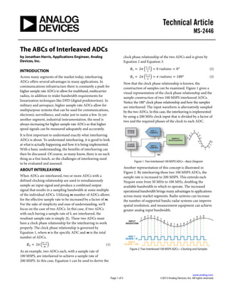
  • 1. Technical Article MS-2446 . www.analog.com Page 1 of 5 ©2013 Analog Devices, Inc. All rights reserved. The ABCs of Interleaved ADCs by Jonathan Harris, Applications Engineer, Analog Devices, Inc. INTRODUCTION Across many segments of the market today, interleaving ADCs offers several advantages in many applications. In communications infrastructure there is constantly a push for higher sample rate ADCs to allow for multiband, multicarrier radios, in addition to wider bandwidth requirements for linearization techniques like DPD (digital predistortion). In military and aerospace, higher sample rate ADCs allow for multipurpose systems that can be used for communications, electronic surveillance, and radar just to name a few. In yet another segment, industrial instrumentation, the need is always increasing for higher sample rate ADCs so that higher speed signals can be measured adequately and accurately. It is first important to understand exactly what interleaving ADCs is about. To understand interleaving, it is good to look at what is actually happening and how it is being implemented. With a basic understanding, the benefits of interleaving can then be discussed. Of course, as many know, there is no such thing as a free lunch, so the challenges of interleaving need to be evaluated and assessed. ABOUT INTERLEAVING When ADCs are interleaved, two or more ADCs with a defined clocking relationship are used to simultaneously sample an input signal and produce a combined output signal that results in a sampling bandwidth at some multiple of the individual ADCs. Utilizing m number of ADCs allows for the effective sample rate to be increased by a factor of m. For the sake of simplicity and ease of understanding, we’ll focus on the case of two ADCs. In this case, if two ADCs with each having a sample rate of fS are interleaved, the resultant sample rate is simply 2fS. These two ADCs must have a clock phase relationship for the interleaving to work properly. The clock phase relationship is governed by Equation 1, where n is the specific ADC and m is the total number of ADCs. ∅ 𝑛 = 2𝜋 � 𝑛−1 𝑚 � (1) As an example, two ADCs each, with a sample rate of 100 MSPS, are interleaved to achieve a sample rate of 200 MSPS. In this case, Equation 1 can be used to derive the clock phase relationship of the two ADCs and is given by Equation 2 and Equation 3. ∅1 = 2𝜋 � 1−1 2 � = 0 𝑟𝑎𝑑𝑖𝑎𝑛𝑠 = 0 𝑜 (2) ∅2 = 2𝜋 � 2−1 2 � = 𝜋 𝑟𝑎𝑑𝑖𝑎𝑛𝑠 = 180 𝑜 (3) Now that the clock phase relationship is known, the construction of samples can be examined. Figure 1 gives a visual representation of the clock phase relationship and the sample construction of two 100 MSPS interleaved ADCs. Notice the 180° clock phase relationship and how the samples are interleaved. The input waveform is alternatively sampled by the two ADCs. In this case, the interleaving is implemented by using a 200 MHz clock input that is divided by a factor of two and the required phases of the clock to each ADC. Figure 1. Two Interleaved 100 MSPS ADCs—Basic Diagram Another representation of this concept is illustrated in Figure 2. By interleaving these two 100 MSPS ADCs, the sample rate is increased to 200 MSPS. This extends each Nyquist zone from 50 MHz to 100 MHz, doubling the available bandwidth in which to operate. The increased operational bandwidth brings many advantages to applications across many market segments. Radio systems can increase the number of supported bands; radar systems can improve spatial resolution, and measurement equipment can achieve greater analog input bandwidth. Figure 2. Two Interleaved 100 MSPS ADCs—Clocking and Samples
  • 2. MS-2446 Technical Article Page 2 of 5 BENEFITS OF INTERLEAVING The benefits of interleaving span across multiple segments of the market. The most desired benefit of interleaving is the increased bandwidth made possible by the wider Nyquist zone of the interleaved ADCs. Once again, taking the example of two 100 MSPS ADCs interleaved to create a sample rate of 200 MSPS, Figure 3 gives a representation of the much wider bandwidth allowed by interleaving the two ADCs. This creates advantages for many different applications. As cellular standards increase channel bandwidth and the number of operating bands, there are increased demands on the available bandwidth in the ADC. In addition, in military applications, the requirements for better spatial recognition, as well as increased channel bandwidths in backend com- munications require higher bandwidths from the ADC. Due to the increased demands for bandwidth in these areas, there is a need created to measure these signals accurately. Therefore, measurement equipment has increased needs for higher bandwidths in order to properly acquire and measure these signals that have higher bandwidth. The system requirements in many designs inherently stay ahead of commercial ADC technology. Interleaving allows for some of this gap to be closed. Figure 3. Two Interleaved ADCs—Nyquist Zone The increased sample rate provides more bandwidth for these applications but also allows for easier frequency planning and reduction in the complexity and cost of the anti-aliasing filter that is typically used at the ADC inputs. With all these great benefits, one has to wonder what the price is to pay. As with most things, there is no such thing as a free lunch. Interleaved ADCs offer increased bandwidth and other nice benefits, but there are some challenges that arise when dealing with interleaved ADCs. CHALLENGES WITH INTERLEAVING There are some challenges and things to look out for when interleaving ADCs. There are spurs that appear in the output spectrum that result from the imperfections associated with interleaving ADCs. These imperfections are basically mismatches between the two ADCs that are being interleaved. There are four basic mismatches that result in spurs in the output spectrum. These are offset mismatch, gain mismatch, timing mismatch, and bandwidth mismatch. The easiest of these to understand is probably the offset mismatch between the two ADCs. Each ADC will have an associated dc offset value. When the two ADCs are interleaved and samples are acquired alternatively back and forth between the two ADCs, the dc offset of each successive sample is changing. Figure 4 gives an example of how each ADC has its own dc offset and how the interleaved output will effectively switch back and forth between these two dc offset values. The output switches between these offset values at a rate of fS/2 which will result in a spur in the output spectrum located at fS/2. Since the mismatch itself does not have a frequency component and is only at dc, the frequency of the spur that appears in the output spectrum only depends on the sampling frequency and will always appear at a frequency of fS/2. The magnitude of the spur is dependent upon the magnitude of the offset mismatch between the ADCs. The greater the mismatch, the larger the spur will be. In order to minimize the spur caused by the offset mismatch, it is not necessary to completely null the dc offset in each ADC. Doing this would filter out any DC content in the signal and would not work for systems using a ZIF (zero IF) architecture where the signal content is real and complex and includes data at DC. Instead, a more appropriate technique would be to match the offset of one of the ADCs to the other ADC. The offset of one ADC is chosen as the reference, and the offset of the other ADC is set to match that value as closely as possible. The better matched the offset values are, the lower the resulting spur is at fS/2. The second mismatch to look at when interleaving is the gain mismatch between the ADCs. Figure 5 gives a representation of the gain mismatch between two interleaved converters. In this case, there is a frequency component to the mismatch. In order to observe this mismatch, there has to be a signal applied to the ADCs. In the case of the offset mismatch, no signal is necessary to see the inherent dc offset of the two ADCs. In the case of the gain mismatch, there is no way to see the gain mismatch unless a signal is present and the gain mismatch can be measured. The gain mismatch will result in a spur in the output spectrum that is related to the input frequency, as well as the sampling rate, and will appear at fS/2 ± fIN. In order to minimize the spur caused by
  • 3. Technical Article MS-2446 Page 3 of 5 the gain mismatch, a similar strategy as what is used for the offset mismatch is employed. The gain of one of the ADCs is chosen as the reference, and the gain of the other ADC is set to match that gain value as closely as possible. The better the gain values of each ADC are matched to each other, the less the resulting spur will be in the output spectrum. Next, we must examine the timing mismatch between the two ADCs. The timing mismatch has two components, group delay in the analog section of the ADC and clock skew. The analog circuitry within the ADC has an associated group delay and the value can be different between the two ADCs. In addition, there is clock skew that has an aperture uncertainty component in each of the ADCs and has a component related to the accuracy of the clock phases that are input to each converter. Figure 6 gives a visual representation of the mechanism and effects of the timing mismatches in the ADCs. Similar to the gain mismatch spur, the timing mismatch spur is also a function of the input frequency and the sample rate and appears at fS/2 ± fIN. In order to minimize the resulting spur, the group delay through the analog section of each converter needs to be properly matched with good circuit design techniques. In addition, the clock path designs need to be closely matched to minimize aperture uncertainty differences. And lastly, the clock phase relationships need to be precisely controlled such that the two input clocks are as close to 180° apart as possible. As with the other mismatches, the goal is to attempt to minimize the mechanisms that cause the timing mismatch. The last mismatch to look at is probably the most difficult to comprehend and handle; it is the bandwidth mismatch. As shown in Figure 7, the bandwidth mismatch has a gain and a phase/frequency component. This makes bandwidth mismatch more difficult because it contains components from two of the other mismatch parameters. In the bandwidth mismatch, however, we see different gain values at different frequencies. In addition, the bandwidth has a timing component which causes signals at different frequencies to have different delays through each converter. The best way to minimize the bandwidth mismatch is to have very good circuit design and layout practices that work to minimize the bandwidth mismatches between the ADCs. The better matched each ADC is, the less the resulting spur will be. Just as the gain and timing mismatches caused spurs in the output spectrum at fS/2 ± fIN, the bandwidth mismatch also results in a spur at the same frequency. Figure 4. Offset Mismatch Figure 5. Gain Mismatch
  • 4. MS-2446 Technical Article Page 4 of 5 Figure 6. Timing Mismatch Figure 7. Bandwidth Mismatch Now that we’ve discussed four different mismatches that cause issues when interleaving ADCs, it is apparent that a commonality has emerged. Three of the four mismatches produce a spur in the output spectrum at fS/2 ± fIN. The offset mismatch spur can be easily identified since it alone resides at fS/2 and can be compensated fairly easily. The gain, timing, and bandwidth mismatches all produce a spur at fS/2 ± fIN in the output spectrum so the question is how to identify the contribution of each. Figure 8 gives a quick visual guide to the process of identifying the sources of the spurs from the different mismatches of interleaved ADCs. Figure 8. Interrelated Nature of Interleaving Mismatches If looking purely at gain mismatch alone, it is a low frequency, or dc, type of mismatch. The gain component of the bandwidth mismatch can be separated from the gain mismatch by performing a gain measurement at low frequency near dc and then performing gain measurements at higher frequencies. The gain mismatch is not a function of frequency like the gain component of the bandwidth mismatch. A similar approach is used for the timing mismatch. A measurement is performed at low frequency near dc and then subsequent measurements are performed at higher frequencies to separate the timing component of bandwidth mismatch from the timing mismatch. CONCLUSION The newest communication system designs, cutting edge radar technologies, and ultrahigh bandwidth measurement equipment seem to constantly outpace the available ADC technology. These requirements push both users and manufacturers of ADCs to develop methods to keep pace with these demands. Interleaving ADCs allows for greater bandwidths to be achieved at a faster pace than the traditional path of increasing the conversion rate of a typical ADC. By taking two or more ADCs and interleaving them together, the available bandwidth is increased, and system design requirements can be met at a faster pace. Interleaving ADCs does not come for free, however, and mismatches between the ADCs cannot be ignored. Even though the mismatches do exist, knowing about them and how to appropriately deal with them can enable designers to use these interleaved ADCs more intelligently and meet the ever increasing demands of their latest system designs.
  • 5. Technical Article MS-2446 Page 5 of 5 REFERENCES Had, Jim, Mark Looney, and Rob Reeder. “Pushing the State of the Art with Mulitchannel A/D Converters.” Analog Dialogue. Vol. 39, No. 5, May 2005. RESOURCES Share this article on One Technology Way • P.O. Box 9106 • Norwood, MA 02062-9106, U.S.A. Tel: 781.329.4700 • Fax: 781.461.3113 • www.analog.com Trademarks and registered trademarks are the property of their respective owners. TA11329-0-1/13 www.analog.com ©2013 Analog Devices, Inc. All rights reserved.