
Recomendados
Más contenido relacionado
La actualidad más candente
La actualidad más candente (18)
Destacado
Destacado (20)
Similar a Tw8804產品
Similar a Tw8804產品 (20)
Último
Último (20)
Tw8804產品
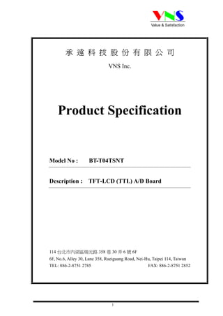
- 1. Value & Satisfaction 承遠科技股份有限公司 VNS Inc. Product Specification Model No : BT-T04TSNT Description : TFT-LCD (TTL) A/D Board 114 台北市內湖區瑞光路 358 巷 30 弄 6 號 6F 6F, No.6, Alley 30, Lane 358, Rueiguang Road, Nei-Hu, Taipei 114, Taiwan TEL: 886-2-8751 2785 FAX: 886-2-8751 2852 1
- 2. Value & Satisfaction TABLE OF CONTENTS NO CONTENTS PAGE 1 General Specification 3 2 Keypad Usage 4 3 OSD Function 5 4 Connectors, Pinouts & Jumpers 5 5 Applicable Graphic Mode 11 6 Tested Panel 11 7 13 Photo of A/D Board 2
- 3. Value & Satisfaction 1. GENERAL SPECIFICATION Scaler Chip Solution TW8804 Graphics Input Analog RGB / FB Input Suppers 3、4、6 or 8 bits per pixel up to 16.8 million colors Number of Colors Analog RGB Supports up to SXGA TTL (Double pixel up to SXGA 75Hz). Panel Output Suppers 3、4、6 or 8 bits Composite Input x2 & S-Video Input x1 & Component Input x1 Signal Input Connector Type OSD Control (Optional) Power , Menu , Left / Down , Right / Up , Exit / Auto Plug & Play VESA DDC 2B compatible +3.3V DC Voltage Output for LCD +12V / +5V DC Input voltage Controller Dimensions 114 x 100 mm Storage temperature limits -20 C to +70 C Operating Temperature 0 C to +60 3
- 4. Value & Satisfaction 2. KEYPAD USAGE 3.1 OSD Board Description INPUT LEFT Menu Auto Power LED RIGHT Buttons Description Power Turn the monitor power ON or OFF. Activate the OSD menu. Menu Enter/confirm the selected option. Activate the volume control. Right/Down/Increase Move the selector to the next option. Increase the gauge value of the selected option. Active volume control. Left/UP/Decrease Move the selector to the previous option. Decrease the gauge value of the selected option. Automatically adjust the clock, phase, H-position and V-position. Auto/Exit Value to the most optimal settings. Use full screen when enabling this function. INPUT Select input sources. 4
- 5. Value & Satisfaction 3. OSD FUNCTION 4. CONNECTORS, PINOUTS & JUMPERS CN2 LCD Panel I/F Connector Used: Related Female Housing:PH0.5 1*50 Pin No. Symbols Description 1 GND Ground for gate drive 2 VCC Digital voltage for gate driver; +3.3V 3 VGL TFT low voltage; -10V 4 VGH TFT high voltage; 15V 5 STVL Start pulse signal input/output (Vertical) 6 STVR Start pulse signal input/output (Vertical) 7 CKV CLK (Vertical) 8 U/D Up or Down display control 9 OEV Output enable 10 VCOM VCOM voltage 11 DIO1 Start pulse signal input/output (Horizontal) 12 AVDD Analog voltage for source driver; +8.4V 13 AVSS Analog ground for source driver 14 GND Digital ground for source driver 15 VCC (DVDD) Digital voltage for source driver; +3.3V 16 EDGSL Select raising edge or raising/falling edge 17 CLK Sample CLK 18 SHL(R/L) Right or Left display control 19 R0 Red data 20 R1 Red data 21 R2 Red data 22 R3 Red data 23 R4 Red data 24 R5 Red data 25 G0 Green Data 26 G1 Green Data 27 G2 Green Data 28 G3 Green Data 29 G4 Green Data 30 G5 Green Data 5
- 6. Value & Satisfaction 31 V1 Reference voltage 32 V2 Reference voltage 33 V3 Reference voltage 34 V4 Reference voltage 35 V5 Reference voltage 36 V6 Reference voltage 37 V7 Reference voltage 38 V8 Reference voltage 39 V9 Reference voltage 40 V10 Reference voltage 41 B0 Blue Data 42 B1 Blue Data 43 B2 Blue Data 44 B3 Blue Data 45 B4 Blue Data 46 B5 Blue Data 47 LD Latch and switch data to output 48 REV Control data are inverted or not 49 POL Polarity selection 50 DIO2 Start pulse signal input/output (Horizontal) 6
- 7. Value & Satisfaction LCD Panel I/F CN3 Connector Used: Relate Male Housing:PH0.5 1*30 FPC Pin No. Symbols Description 1 POL Polarity selection 2 DIO2 Start pulse signal input/output (Vertical) 3 OEV Output enable 4 CKV CLK (Vertical) 5 DIO1 Start pulse signal input/output (Vertical) 6 GND Power Ground 7 EDGSL Select raising edge or raising/falling edge 8 VCC Digital voltage for source driver 9 V9 Gamma voltage level 9 10 VGL Gate OFF voltage 11 V2 Gamma voltage level 2 12 VGH Gate ON voltage 13 V6 Gamma voltage level 6 14 U/D Up or Down display control 15 VCOM Common voltage 16 GND Power Ground 17 AVDD1 Power supply for analog circuit 18 V14 Gamma voltage level 14 19 V11 Gamma voltage level 11 20 V8 Gamma voltage level 8 21 V5 Gamma voltage level 5 22 V3 Gamma voltage level 3 23 GND Power Ground 24 R5 Red data 25 R4 Red data 26 R3 Red data 27 R2 Red data 28 R1 Red data 29 R0 Red data 30 GND Power Ground 7
- 8. Value & Satisfaction CN4 LCD Panel I/F Connector Used: Relate Male Housing:PH0.5 1*30 FPC Pin No. Symbols Description 1 GND Power Ground 2 G5 Green data 3 G4 Green data 4 G3 Green data 5 G2 Green data 6 G1 Green data 7 G0 Green data 8 STHL Start pulse signal input/output (Horizontal) 9 REV Control data are inverted or not 10 GND Power Ground 11 DCLK Sample clock 12 DVDD Voltage for digital circuit 13 STHR Start pulse signal input/output (Horizontal) 14 LD(OEH) Latch and switch data to output 15 B5 Blue data 16 B4 Blue data 17 B3 Blue data 18 B2 Blue data 19 B1 Blue data 20 B0 Blue data 21 L/R Right or Left display control 22 V1 Gamma voltage level 1 23 V4 Gamma voltage level 4 24 V7 Gamma voltage level 7 25 V10 Gamma voltage level 10 26 V12 Gamma voltage level 12 27 V13 Gamma voltage level 13 28 AVDD2 Power supply for analog circuit 29 GND Power Ground 30 VCOM Common voltage 8
- 9. Value & Satisfaction Connector for inverter CON7 Connector Used: Relate female housing:PH1.25 1*6 Wafer Pin No. Symbols Description Output for inverter on/off control 1 CCFL_EN +3.3V ON 0V OFF 2 PWM0 Brightness voltage Control 3 GND Ground 4 GND Ground 5 +12V +12V output for inverter board 6 +12V +12V output for inverter board CON5 Connector for +5V Output Connector Used: Relate female housing:PH1.25 1*2 Wafer Pin No. Symbols Description 1 +5V +5V output for extra device 2 GND Ground CON2 Key pad control Connector Used: Relate female housing:PH1.25 1*9 Wafer Description Pin No. Symbols 1 NC 2 LED2 Output terminal for red color LED indicator 3 LED1 Output terminal for amber color LED indicator 4 GROUND Ground 5 LEFT Left 6 MENU Menu 7 RIGHT Right 8 AUTO Auto adjustment/ Exit 9 POWER ON Power on/off switch 9
- 10. Value & Satisfaction P1 DC Jack for Power Supply Connector Used: Relate Female Housing:DC JACK 2.5Φ Pin No. Symbols Description 1 GND Ground 2 +12V +12V DC power input. 3 GND Ground P2 S-VIDEO Connector Used: Relate Female Housing:MINI DIN 4P Pin No. Symbols Description 1 GND Ground 2 GND Ground 3 Y1N10 S-VIDEO_Y 4 C1N1 S-VIDEO_C Connector for Component CON9 Connector Used: Relate Female Housing:PH1.5 1*6 Wafer Pin No. Symbols Description 1 RIN CR 2 GND Ground 3 GIN Y 4 GND Ground 5 BIN CB 6 GND Ground 10
- 11. Value & Satisfaction CON8 : Connector for Composite Input/Output Connector Used: Relate Female Housing:PH1.5 1*9 Wafer Pin No. Symbols Description 1 CIN1 S-VIDEO_C 2 YIN10 S-VIDEO_Y 3 GND Ground 4 AVOUT VIDEO Output 5 GND Ground 6 YIN11 CVBS 1 7 GND Ground 8 YIN12 CVBS 2 9 GND Ground J2 DC Jack for Power Supply Connector Used: Relate Female Housing:PH2.0 1*2 Header Pin No. Symbols Description 1 GND Ground 2 AVOUT VIDEO Output 3 GND Ground 4 Y1N11 CVBS 1 5 GND Ground 6 Y1N12 CVBS 2 11
- 12. Value & Satisfaction 5. APPLICABLE GRAPHIC TABLE Mode H Freq(KHz) V Freq(Hz) 640·350@70hz +31.500 -70.100 640·480@67hz -35.000 -66.700 640·480@60hz -31.469 -59.9404 640·480@72hz -37.816 -72.809 640·480@75hz -37.500 -75.000 720·400@70hz -31.500 +70.100 800·600@56hz +35.156 +56.250 800·600@60hz +37.900 +60.300 800·600@72hz +48.100 +72.000 800·600@75hz +46.880 +75.000 6. TESTED PANEL This board can support various LCD panels, which have VGA, SVGA and XGA resolution. The table below shows the information of LCD panel. Input Voltage Frequency Signal Manufacture Size Model No. Resolution (Hz) VDD Interface AU 10.2” A102VW01 +3.3V 800x600 75 TTL AU 7” A070VW01 +3.3V 800x600 75 TTL 12
- 13. Value & Satisfaction 7. Photo of A/D Board 13