SlideShare una empresa de Scribd logo
1 de 56
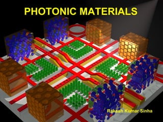
PHOTONIC MATERIALS Rakesh Kumar Sinha
Photonics ,[object Object]
Why Do We Need Photonics instead of Electronics? ,[object Object],[object Object],[object Object],[object Object]
Photonic Crystals Principles and Applications
SO WHAT ARE PHOTONIC CRYSTALS ?   ,[object Object],[object Object]
Photonic crystal with a complete band gap when index contrast is large enough
Features of a photonic crystal ,[object Object]
In  2D photonic crystal  structures it is possible to confine light within a  cavity . Photonic band gaps appear in the plane of periodicity and in 2D  we can achieve  linear localization . By introducing a defect, i.e. removing one column, we may obtain a peak in the density of states localized in the photonic band gap – similar to semiconductors. The defect mode cannot penetrate the crystal in the xy-plane because of the band gap but extends in the z-direction
Photonic Crystals The Principle with photonic band gaps: “ optical insulators ” “ magical oven mitts”  for holding and controlling light can trap light in  cavities and  waveguides  (“wires”)
Photonic Crystals The Principle ,[object Object],[object Object]
Analogy with semiconductors ,[object Object],[object Object],1D
Photonic band gap crystals -- a history   ,[object Object],[object Object]
Photonic Band Gaps ,[object Object],[object Object],[object Object]
[object Object]
Properties of Photonic Crystals
Negative Refraction opposite of   ordinary lens: only   images close objects does   not   require curved   lens can   exceed   classical diffraction limit
Properties of Photonic Crystals
Properties of Photonic Materials: Why no Scattering?? forbidden by gap (except for   finite- crystal   tunneling ) forbidden by Bloch ( k  conserved)
Properties of Photonic Crystals
Properties of Photonic Crystals: Wide Angle Splitters
Applications Of Photonic Crystals ,[object Object],[object Object]
Applications Of Photonic Crystals ,[object Object],A part of Photonic integrated circuit
Applications Of Photonic Crystals ,[object Object]
Imaging by a Flat Slab of  Photonic crystal ,[object Object],[object Object],[object Object],[object Object],[object Object],[object Object],Scale Intensity:  -20 dB to -40 dB X-Y: 37.5 X 30 cm 2
Self organized Nano Photonic Crystal  Negative refraction in Photonic Crystal 3D IMAGING IN REAL SPACE Semiconductor substrate
Flat lens n = -1 d d = u + v v u object image Normal lens: Resolution cannot be greater than   Flat lens : no limitation on the resolution Image resolution Normal lens
E H H E PIM PIM Turning light on its Head Positive Refraction PIM NIM E H E H Negative Refraction
Conventional Optical lens   Photonic Crystal lens Advantages of Photonic Crystal lens Optical axis Limited aperture cannot NO Optical axis No limitation on aperture size Subwavelength imaging (evanescent wave amplification) PC : Scalability  to sub-micron dimensions -> applications at  optical frequencies
Applications Of Photonic Crystals ,[object Object],[object Object]
Applications Of Photonic Crystals Replacing conventional optical fibres The Glass Ceiling :  Limits of Silica Loss : amplifiers every 50–100km … cannot use “exotic” wavelengths like  10.6µm Nonlinearities :  after ~100km, cause dispersion, crosstalk, power limits (limited by mode area ~ single-mode, bending loss) also cannot be made (very) large for compact nonlinear devices Radical modifications to dispersion, polarization effects …tunability  is  limited Long  Distances High Bit-Rates Dense  Wavelength Multiplexing   (DWDM) Compact Devices
Future Applications ,[object Object],[object Object],[object Object],[object Object],[object Object],[object Object],[object Object]
Fabrication Of Photonic Crystals An example of a two-dimensional photonic crystal. The distance between the 200 nm wide pillars is about 500 nm and the pillars are 1500 nm long.
Fabrication Of Photonic Crystals Waveguide bend in a two-dimensional array of rods. The waveguide bend is defined by removing a row rods.
Fabrication Of Photonic Crystals Microfabrication :  By layer by layer lithography. Colloidal self-assembly.
Fabrication Of Photonic Crystals ,[object Object],Layer-by-Layer Lithography •  Fabrication of   2d patterns in Si or GaAs is very advanced (think: Pentium IV, 50 million transistors) So, make 3d structure one layer at a time
 
The Woodpile
Lithography ,[object Object],[object Object],[object Object],[object Object],[object Object],[object Object],[object Object],[object Object]
 
[object Object],[object Object],[object Object],[object Object],[object Object],[object Object],[object Object],Lithography (contd.) The lithographic sequence is repeated for each physical layer
2µm Lithography at its best    = 780nm resolution = 150nm 7µm (3 hours to make)
Lithography at its best 2µm ( 300nm diameter   coils, suspended in ethanol,   viscosity-damped )
Lithography at its best
Mass Production by Holographic Lithography absorptive material Four beams   make 3d-periodic interference pattern (1.4µm) k -vector differences   give reciprocal lattice vectors ( i.e.  periodicity) beam polarizations + amplitudes (8 parameters) give unit cell
Holographic Lithography :The Results huge volumes ,  long-range periodic,   fcc   lattice…
Mass Production :Colloids microspheres  (diameter < 1µm) silica   (SiO 2 ) sediment  by gravity into close-packed   fcc lattice ! (evaporate)
Inverse Opals fcc solid spheres do not have a gap…   … but fcc spherical   holes in Si  do  have a gap [ figs courtesy D. Norris, UMN ] Infiltration sub-micron colloidal spheres Template (synthetic opal) 3D Remove Template “ Inverted Opal”
In Order To Form a More Perfect Crystal… meniscus silica 250nm ,[object Object],[object Object],Heat Source 80C 65C 1 micron  silica spheres in ethanol evaporate  solvent
A Better Opal
Inverse-Opal Photonic Crystal
Manufacturing Photonic Materials: The Biological Option   ,[object Object],[object Object],The  Mitoura Grynea   butterfly   Electron micrograph of a broken scale taken from  mitoura grynea  revealing a periodic array of holes responsible for the colour
Recent Developments (taking it a step ahead) ,[object Object],The picture depicts waveguide bend exhibiting 100% transmission
Recent Developments (taking it a step ahead) ,[object Object],[object Object],[object Object]
Recent Developments (taking it a step ahead) ,[object Object]
Recent Developments (taking it a step ahead) ,[object Object],[object Object],This image shows the microscopic structure of a three-dimensional photonic crystal that is capable of channeling and emitting light in the visible and telecommunications ranges .
THANK  YOU !!!

Más contenido relacionado

La actualidad más candente

La actualidad más candente (20)

Photonics devices
Photonics devicesPhotonics devices
Photonics devices
 
Molecular beam epitaxy
Molecular beam epitaxyMolecular beam epitaxy
Molecular beam epitaxy
 
Pulse laser deposition of thin film
Pulse laser deposition of thin filmPulse laser deposition of thin film
Pulse laser deposition of thin film
 
E beam lithography
E beam lithographyE beam lithography
E beam lithography
 
Focused ion beam lithography
Focused ion beam lithographyFocused ion beam lithography
Focused ion beam lithography
 
Photodetectors
PhotodetectorsPhotodetectors
Photodetectors
 
Synthesis of graphene
Synthesis of grapheneSynthesis of graphene
Synthesis of graphene
 
Examples of Photonics Applications for DAY OF PHOTONICS 21 October 2014
Examples of Photonics Applications for DAY OF PHOTONICS 21 October 2014Examples of Photonics Applications for DAY OF PHOTONICS 21 October 2014
Examples of Photonics Applications for DAY OF PHOTONICS 21 October 2014
 
Lecture 21
Lecture 21Lecture 21
Lecture 21
 
organic solar cell
organic solar cellorganic solar cell
organic solar cell
 
Preparation of thin films
Preparation of thin filmsPreparation of thin films
Preparation of thin films
 
Introduction to nanophotonics
Introduction to nanophotonicsIntroduction to nanophotonics
Introduction to nanophotonics
 
Nano lithography techniques
Nano lithography techniquesNano lithography techniques
Nano lithography techniques
 
Photo-detector by GIRISH HARMUKH
Photo-detector by GIRISH HARMUKHPhoto-detector by GIRISH HARMUKH
Photo-detector by GIRISH HARMUKH
 
PHOTONIC DEVICES INTRODUCTION
PHOTONIC DEVICES INTRODUCTIONPHOTONIC DEVICES INTRODUCTION
PHOTONIC DEVICES INTRODUCTION
 
Lithography fabrication ppt
Lithography fabrication pptLithography fabrication ppt
Lithography fabrication ppt
 
quantum dots
quantum dotsquantum dots
quantum dots
 
Photonic crystal fibers (PCF)
Photonic crystal fibers (PCF)Photonic crystal fibers (PCF)
Photonic crystal fibers (PCF)
 
Semiconductor Nanomaterials
Semiconductor NanomaterialsSemiconductor Nanomaterials
Semiconductor Nanomaterials
 
Electrodeposited Ni- Based nano composites
Electrodeposited Ni- Based nano compositesElectrodeposited Ni- Based nano composites
Electrodeposited Ni- Based nano composites
 

Similar a Photonic Materials

Photonics Metamaterials
Photonics MetamaterialsPhotonics Metamaterials
Photonics MetamaterialsPraveen Sharma
 
My Final Year Project Final Report.pptx
My Final Year Project Final Report.pptxMy Final Year Project Final Report.pptx
My Final Year Project Final Report.pptxSanjayKumarSingh642747
 
Report In Japan 20060613 Liuxu
Report In Japan 20060613 LiuxuReport In Japan 20060613 Liuxu
Report In Japan 20060613 Liuxu巍 陆
 
LASER,FIBER OPTICS & ULTRASONIC……
LASER,FIBER OPTICS  & ULTRASONIC……LASER,FIBER OPTICS  & ULTRASONIC……
LASER,FIBER OPTICS & ULTRASONIC……Smit Shah
 
Opal and inverse opal structures for optical device applications
Opal and inverse opal structures for optical device applicationsOpal and inverse opal structures for optical device applications
Opal and inverse opal structures for optical device applicationsM. Faisal Halim
 
Microscopy by S.D.Mankar, Assistant Professor, Department of Pharmaceutics, P...
Microscopy by S.D.Mankar, Assistant Professor, Department of Pharmaceutics, P...Microscopy by S.D.Mankar, Assistant Professor, Department of Pharmaceutics, P...
Microscopy by S.D.Mankar, Assistant Professor, Department of Pharmaceutics, P...someshwar mankar
 
Traineeship Melbourne University - Michael Beljaars
Traineeship Melbourne University - Michael BeljaarsTraineeship Melbourne University - Michael Beljaars
Traineeship Melbourne University - Michael BeljaarsMichael Beljaars
 
Optical fiber by debraj maji
Optical fiber by debraj majiOptical fiber by debraj maji
Optical fiber by debraj majiDebraj Maji
 
Electron beam lithography
Electron beam lithographyElectron beam lithography
Electron beam lithographyRohan Deokar
 
Microscopy by S.D.Mankar, Assistant Professor, Department of Pharmaceutics, P...
Microscopy by S.D.Mankar, Assistant Professor, Department of Pharmaceutics, P...Microscopy by S.D.Mankar, Assistant Professor, Department of Pharmaceutics, P...
Microscopy by S.D.Mankar, Assistant Professor, Department of Pharmaceutics, P...someshwar mankar
 
Nano meta materials
Nano   meta materialsNano   meta materials
Nano meta materialsHemant Kumar
 

Similar a Photonic Materials (20)

Photonics Metamaterials
Photonics MetamaterialsPhotonics Metamaterials
Photonics Metamaterials
 
My Final Year Project Final Report.pptx
My Final Year Project Final Report.pptxMy Final Year Project Final Report.pptx
My Final Year Project Final Report.pptx
 
Report In Japan 20060613 Liuxu
Report In Japan 20060613 LiuxuReport In Japan 20060613 Liuxu
Report In Japan 20060613 Liuxu
 
Pc laser
Pc laserPc laser
Pc laser
 
LASER,FIBER OPTICS & ULTRASONIC……
LASER,FIBER OPTICS  & ULTRASONIC……LASER,FIBER OPTICS  & ULTRASONIC……
LASER,FIBER OPTICS & ULTRASONIC……
 
Opal and inverse opal structures for optical device applications
Opal and inverse opal structures for optical device applicationsOpal and inverse opal structures for optical device applications
Opal and inverse opal structures for optical device applications
 
Optical fiber
Optical fiberOptical fiber
Optical fiber
 
PHOTONIC CRYSTALS,.pptx
PHOTONIC CRYSTALS,.pptxPHOTONIC CRYSTALS,.pptx
PHOTONIC CRYSTALS,.pptx
 
Otago 2019 1
Otago 2019 1Otago 2019 1
Otago 2019 1
 
Microscopy by S.D.Mankar, Assistant Professor, Department of Pharmaceutics, P...
Microscopy by S.D.Mankar, Assistant Professor, Department of Pharmaceutics, P...Microscopy by S.D.Mankar, Assistant Professor, Department of Pharmaceutics, P...
Microscopy by S.D.Mankar, Assistant Professor, Department of Pharmaceutics, P...
 
Traineeship Melbourne University - Michael Beljaars
Traineeship Melbourne University - Michael BeljaarsTraineeship Melbourne University - Michael Beljaars
Traineeship Melbourne University - Michael Beljaars
 
Study of Optical Character of Nano-antenna
Study of Optical Character of Nano-antennaStudy of Optical Character of Nano-antenna
Study of Optical Character of Nano-antenna
 
Abstract
AbstractAbstract
Abstract
 
Optical fiber by debraj maji
Optical fiber by debraj majiOptical fiber by debraj maji
Optical fiber by debraj maji
 
Nantenna
NantennaNantenna
Nantenna
 
Electron beam lithography
Electron beam lithographyElectron beam lithography
Electron beam lithography
 
Microscopy by S.D.Mankar, Assistant Professor, Department of Pharmaceutics, P...
Microscopy by S.D.Mankar, Assistant Professor, Department of Pharmaceutics, P...Microscopy by S.D.Mankar, Assistant Professor, Department of Pharmaceutics, P...
Microscopy by S.D.Mankar, Assistant Professor, Department of Pharmaceutics, P...
 
Approaches of nanoelectronics
Approaches of nanoelectronicsApproaches of nanoelectronics
Approaches of nanoelectronics
 
Nano meta materials
Nano   meta materialsNano   meta materials
Nano meta materials
 
U01061151154
U01061151154U01061151154
U01061151154
 

Más de Gaurav Singh Chandel (8)

Building materials
Building materialsBuilding materials
Building materials
 
Material parameter modeling
Material parameter modelingMaterial parameter modeling
Material parameter modeling
 
Honeycomb Carbon Materials
Honeycomb  Carbon MaterialsHoneycomb  Carbon Materials
Honeycomb Carbon Materials
 
Eukariotic Cell Structure
Eukariotic Cell StructureEukariotic Cell Structure
Eukariotic Cell Structure
 
Bacterial Cell
Bacterial CellBacterial Cell
Bacterial Cell
 
conducting polymers
conducting polymersconducting polymers
conducting polymers
 
Nanotechnology Applied To Life Sciences
Nanotechnology Applied To Life SciencesNanotechnology Applied To Life Sciences
Nanotechnology Applied To Life Sciences
 
Deadlock
DeadlockDeadlock
Deadlock
 

Último

Grateful 7 speech thanking everyone that has helped.pdf
Grateful 7 speech thanking everyone that has helped.pdfGrateful 7 speech thanking everyone that has helped.pdf
Grateful 7 speech thanking everyone that has helped.pdfPaul Menig
 
Call Girls in Mehrauli Delhi 💯Call Us 🔝8264348440🔝
Call Girls in Mehrauli Delhi 💯Call Us 🔝8264348440🔝Call Girls in Mehrauli Delhi 💯Call Us 🔝8264348440🔝
Call Girls in Mehrauli Delhi 💯Call Us 🔝8264348440🔝soniya singh
 
Call Girls In Radisson Blu Hotel New Delhi Paschim Vihar ❤️8860477959 Escorts...
Call Girls In Radisson Blu Hotel New Delhi Paschim Vihar ❤️8860477959 Escorts...Call Girls In Radisson Blu Hotel New Delhi Paschim Vihar ❤️8860477959 Escorts...
Call Girls In Radisson Blu Hotel New Delhi Paschim Vihar ❤️8860477959 Escorts...lizamodels9
 
Call Girls In Sikandarpur Gurgaon ❤️8860477959_Russian 100% Genuine Escorts I...
Call Girls In Sikandarpur Gurgaon ❤️8860477959_Russian 100% Genuine Escorts I...Call Girls In Sikandarpur Gurgaon ❤️8860477959_Russian 100% Genuine Escorts I...
Call Girls In Sikandarpur Gurgaon ❤️8860477959_Russian 100% Genuine Escorts I...lizamodels9
 
VIP Call Girl Jamshedpur Aashi 8250192130 Independent Escort Service Jamshedpur
VIP Call Girl Jamshedpur Aashi 8250192130 Independent Escort Service JamshedpurVIP Call Girl Jamshedpur Aashi 8250192130 Independent Escort Service Jamshedpur
VIP Call Girl Jamshedpur Aashi 8250192130 Independent Escort Service JamshedpurSuhani Kapoor
 
7.pdf This presentation captures many uses and the significance of the number...
7.pdf This presentation captures many uses and the significance of the number...7.pdf This presentation captures many uses and the significance of the number...
7.pdf This presentation captures many uses and the significance of the number...Paul Menig
 
Marketing Management Business Plan_My Sweet Creations
Marketing Management Business Plan_My Sweet CreationsMarketing Management Business Plan_My Sweet Creations
Marketing Management Business Plan_My Sweet Creationsnakalysalcedo61
 
VIP Kolkata Call Girl Howrah 👉 8250192130 Available With Room
VIP Kolkata Call Girl Howrah 👉 8250192130  Available With RoomVIP Kolkata Call Girl Howrah 👉 8250192130  Available With Room
VIP Kolkata Call Girl Howrah 👉 8250192130 Available With Roomdivyansh0kumar0
 
Vip Dewas Call Girls #9907093804 Contact Number Escorts Service Dewas
Vip Dewas Call Girls #9907093804 Contact Number Escorts Service DewasVip Dewas Call Girls #9907093804 Contact Number Escorts Service Dewas
Vip Dewas Call Girls #9907093804 Contact Number Escorts Service Dewasmakika9823
 
Keppel Ltd. 1Q 2024 Business Update Presentation Slides
Keppel Ltd. 1Q 2024 Business Update  Presentation SlidesKeppel Ltd. 1Q 2024 Business Update  Presentation Slides
Keppel Ltd. 1Q 2024 Business Update Presentation SlidesKeppelCorporation
 
BEST Call Girls In Greater Noida ✨ 9773824855 ✨ Escorts Service In Delhi Ncr,
BEST Call Girls In Greater Noida ✨ 9773824855 ✨ Escorts Service In Delhi Ncr,BEST Call Girls In Greater Noida ✨ 9773824855 ✨ Escorts Service In Delhi Ncr,
BEST Call Girls In Greater Noida ✨ 9773824855 ✨ Escorts Service In Delhi Ncr,noida100girls
 
Catalogue ONG NUOC PPR DE NHAT .pdf
Catalogue ONG NUOC PPR DE NHAT      .pdfCatalogue ONG NUOC PPR DE NHAT      .pdf
Catalogue ONG NUOC PPR DE NHAT .pdfOrient Homes
 
Regression analysis: Simple Linear Regression Multiple Linear Regression
Regression analysis:  Simple Linear Regression Multiple Linear RegressionRegression analysis:  Simple Linear Regression Multiple Linear Regression
Regression analysis: Simple Linear Regression Multiple Linear RegressionRavindra Nath Shukla
 
Call Girls in Gomti Nagar - 7388211116 - With room Service
Call Girls in Gomti Nagar - 7388211116  - With room ServiceCall Girls in Gomti Nagar - 7388211116  - With room Service
Call Girls in Gomti Nagar - 7388211116 - With room Servicediscovermytutordmt
 
/:Call Girls In Jaypee Siddharth - 5 Star Hotel New Delhi ➥9990211544 Top Esc...
/:Call Girls In Jaypee Siddharth - 5 Star Hotel New Delhi ➥9990211544 Top Esc.../:Call Girls In Jaypee Siddharth - 5 Star Hotel New Delhi ➥9990211544 Top Esc...
/:Call Girls In Jaypee Siddharth - 5 Star Hotel New Delhi ➥9990211544 Top Esc...lizamodels9
 
Lean: From Theory to Practice — One City’s (and Library’s) Lean Story… Abridged
Lean: From Theory to Practice — One City’s (and Library’s) Lean Story… AbridgedLean: From Theory to Practice — One City’s (and Library’s) Lean Story… Abridged
Lean: From Theory to Practice — One City’s (and Library’s) Lean Story… AbridgedKaiNexus
 
Eni 2024 1Q Results - 24.04.24 business.
Eni 2024 1Q Results - 24.04.24 business.Eni 2024 1Q Results - 24.04.24 business.
Eni 2024 1Q Results - 24.04.24 business.Eni
 
VIP Call Girls Pune Kirti 8617697112 Independent Escort Service Pune
VIP Call Girls Pune Kirti 8617697112 Independent Escort Service PuneVIP Call Girls Pune Kirti 8617697112 Independent Escort Service Pune
VIP Call Girls Pune Kirti 8617697112 Independent Escort Service PuneCall girls in Ahmedabad High profile
 

Último (20)

Grateful 7 speech thanking everyone that has helped.pdf
Grateful 7 speech thanking everyone that has helped.pdfGrateful 7 speech thanking everyone that has helped.pdf
Grateful 7 speech thanking everyone that has helped.pdf
 
Call Girls in Mehrauli Delhi 💯Call Us 🔝8264348440🔝
Call Girls in Mehrauli Delhi 💯Call Us 🔝8264348440🔝Call Girls in Mehrauli Delhi 💯Call Us 🔝8264348440🔝
Call Girls in Mehrauli Delhi 💯Call Us 🔝8264348440🔝
 
Call Girls In Radisson Blu Hotel New Delhi Paschim Vihar ❤️8860477959 Escorts...
Call Girls In Radisson Blu Hotel New Delhi Paschim Vihar ❤️8860477959 Escorts...Call Girls In Radisson Blu Hotel New Delhi Paschim Vihar ❤️8860477959 Escorts...
Call Girls In Radisson Blu Hotel New Delhi Paschim Vihar ❤️8860477959 Escorts...
 
Call Girls In Sikandarpur Gurgaon ❤️8860477959_Russian 100% Genuine Escorts I...
Call Girls In Sikandarpur Gurgaon ❤️8860477959_Russian 100% Genuine Escorts I...Call Girls In Sikandarpur Gurgaon ❤️8860477959_Russian 100% Genuine Escorts I...
Call Girls In Sikandarpur Gurgaon ❤️8860477959_Russian 100% Genuine Escorts I...
 
VIP Call Girl Jamshedpur Aashi 8250192130 Independent Escort Service Jamshedpur
VIP Call Girl Jamshedpur Aashi 8250192130 Independent Escort Service JamshedpurVIP Call Girl Jamshedpur Aashi 8250192130 Independent Escort Service Jamshedpur
VIP Call Girl Jamshedpur Aashi 8250192130 Independent Escort Service Jamshedpur
 
7.pdf This presentation captures many uses and the significance of the number...
7.pdf This presentation captures many uses and the significance of the number...7.pdf This presentation captures many uses and the significance of the number...
7.pdf This presentation captures many uses and the significance of the number...
 
Marketing Management Business Plan_My Sweet Creations
Marketing Management Business Plan_My Sweet CreationsMarketing Management Business Plan_My Sweet Creations
Marketing Management Business Plan_My Sweet Creations
 
VIP Kolkata Call Girl Howrah 👉 8250192130 Available With Room
VIP Kolkata Call Girl Howrah 👉 8250192130  Available With RoomVIP Kolkata Call Girl Howrah 👉 8250192130  Available With Room
VIP Kolkata Call Girl Howrah 👉 8250192130 Available With Room
 
Vip Dewas Call Girls #9907093804 Contact Number Escorts Service Dewas
Vip Dewas Call Girls #9907093804 Contact Number Escorts Service DewasVip Dewas Call Girls #9907093804 Contact Number Escorts Service Dewas
Vip Dewas Call Girls #9907093804 Contact Number Escorts Service Dewas
 
KestrelPro Flyer Japan IT Week 2024 (English)
KestrelPro Flyer Japan IT Week 2024 (English)KestrelPro Flyer Japan IT Week 2024 (English)
KestrelPro Flyer Japan IT Week 2024 (English)
 
Keppel Ltd. 1Q 2024 Business Update Presentation Slides
Keppel Ltd. 1Q 2024 Business Update  Presentation SlidesKeppel Ltd. 1Q 2024 Business Update  Presentation Slides
Keppel Ltd. 1Q 2024 Business Update Presentation Slides
 
BEST Call Girls In Greater Noida ✨ 9773824855 ✨ Escorts Service In Delhi Ncr,
BEST Call Girls In Greater Noida ✨ 9773824855 ✨ Escorts Service In Delhi Ncr,BEST Call Girls In Greater Noida ✨ 9773824855 ✨ Escorts Service In Delhi Ncr,
BEST Call Girls In Greater Noida ✨ 9773824855 ✨ Escorts Service In Delhi Ncr,
 
Catalogue ONG NUOC PPR DE NHAT .pdf
Catalogue ONG NUOC PPR DE NHAT      .pdfCatalogue ONG NUOC PPR DE NHAT      .pdf
Catalogue ONG NUOC PPR DE NHAT .pdf
 
Regression analysis: Simple Linear Regression Multiple Linear Regression
Regression analysis:  Simple Linear Regression Multiple Linear RegressionRegression analysis:  Simple Linear Regression Multiple Linear Regression
Regression analysis: Simple Linear Regression Multiple Linear Regression
 
Call Girls in Gomti Nagar - 7388211116 - With room Service
Call Girls in Gomti Nagar - 7388211116  - With room ServiceCall Girls in Gomti Nagar - 7388211116  - With room Service
Call Girls in Gomti Nagar - 7388211116 - With room Service
 
/:Call Girls In Jaypee Siddharth - 5 Star Hotel New Delhi ➥9990211544 Top Esc...
/:Call Girls In Jaypee Siddharth - 5 Star Hotel New Delhi ➥9990211544 Top Esc.../:Call Girls In Jaypee Siddharth - 5 Star Hotel New Delhi ➥9990211544 Top Esc...
/:Call Girls In Jaypee Siddharth - 5 Star Hotel New Delhi ➥9990211544 Top Esc...
 
Best Practices for Implementing an External Recruiting Partnership
Best Practices for Implementing an External Recruiting PartnershipBest Practices for Implementing an External Recruiting Partnership
Best Practices for Implementing an External Recruiting Partnership
 
Lean: From Theory to Practice — One City’s (and Library’s) Lean Story… Abridged
Lean: From Theory to Practice — One City’s (and Library’s) Lean Story… AbridgedLean: From Theory to Practice — One City’s (and Library’s) Lean Story… Abridged
Lean: From Theory to Practice — One City’s (and Library’s) Lean Story… Abridged
 
Eni 2024 1Q Results - 24.04.24 business.
Eni 2024 1Q Results - 24.04.24 business.Eni 2024 1Q Results - 24.04.24 business.
Eni 2024 1Q Results - 24.04.24 business.
 
VIP Call Girls Pune Kirti 8617697112 Independent Escort Service Pune
VIP Call Girls Pune Kirti 8617697112 Independent Escort Service PuneVIP Call Girls Pune Kirti 8617697112 Independent Escort Service Pune
VIP Call Girls Pune Kirti 8617697112 Independent Escort Service Pune
 

Photonic Materials

  • 2.
  • 3.
  • 4. Photonic Crystals Principles and Applications
  • 5.
  • 6. Photonic crystal with a complete band gap when index contrast is large enough
  • 7.
  • 8. In 2D photonic crystal structures it is possible to confine light within a cavity . Photonic band gaps appear in the plane of periodicity and in 2D we can achieve linear localization . By introducing a defect, i.e. removing one column, we may obtain a peak in the density of states localized in the photonic band gap – similar to semiconductors. The defect mode cannot penetrate the crystal in the xy-plane because of the band gap but extends in the z-direction
  • 9. Photonic Crystals The Principle with photonic band gaps: “ optical insulators ” “ magical oven mitts” for holding and controlling light can trap light in cavities and waveguides (“wires”)
  • 10.
  • 11.
  • 12.
  • 13.
  • 14.
  • 16. Negative Refraction opposite of ordinary lens: only images close objects does not require curved lens can exceed classical diffraction limit
  • 18. Properties of Photonic Materials: Why no Scattering?? forbidden by gap (except for finite- crystal tunneling ) forbidden by Bloch ( k conserved)
  • 20. Properties of Photonic Crystals: Wide Angle Splitters
  • 21.
  • 22.
  • 23.
  • 24.
  • 25. Self organized Nano Photonic Crystal Negative refraction in Photonic Crystal 3D IMAGING IN REAL SPACE Semiconductor substrate
  • 26. Flat lens n = -1 d d = u + v v u object image Normal lens: Resolution cannot be greater than  Flat lens : no limitation on the resolution Image resolution Normal lens
  • 27. E H H E PIM PIM Turning light on its Head Positive Refraction PIM NIM E H E H Negative Refraction
  • 28. Conventional Optical lens Photonic Crystal lens Advantages of Photonic Crystal lens Optical axis Limited aperture cannot NO Optical axis No limitation on aperture size Subwavelength imaging (evanescent wave amplification) PC : Scalability to sub-micron dimensions -> applications at optical frequencies
  • 29.
  • 30. Applications Of Photonic Crystals Replacing conventional optical fibres The Glass Ceiling : Limits of Silica Loss : amplifiers every 50–100km … cannot use “exotic” wavelengths like 10.6µm Nonlinearities : after ~100km, cause dispersion, crosstalk, power limits (limited by mode area ~ single-mode, bending loss) also cannot be made (very) large for compact nonlinear devices Radical modifications to dispersion, polarization effects …tunability is limited Long Distances High Bit-Rates Dense Wavelength Multiplexing (DWDM) Compact Devices
  • 31.
  • 32. Fabrication Of Photonic Crystals An example of a two-dimensional photonic crystal. The distance between the 200 nm wide pillars is about 500 nm and the pillars are 1500 nm long.
  • 33. Fabrication Of Photonic Crystals Waveguide bend in a two-dimensional array of rods. The waveguide bend is defined by removing a row rods.
  • 34. Fabrication Of Photonic Crystals Microfabrication : By layer by layer lithography. Colloidal self-assembly.
  • 35.
  • 36.  
  • 38.
  • 39.  
  • 40.
  • 41. 2µm Lithography at its best  = 780nm resolution = 150nm 7µm (3 hours to make)
  • 42. Lithography at its best 2µm ( 300nm diameter coils, suspended in ethanol, viscosity-damped )
  • 44. Mass Production by Holographic Lithography absorptive material Four beams make 3d-periodic interference pattern (1.4µm) k -vector differences give reciprocal lattice vectors ( i.e. periodicity) beam polarizations + amplitudes (8 parameters) give unit cell
  • 45. Holographic Lithography :The Results huge volumes , long-range periodic, fcc lattice…
  • 46. Mass Production :Colloids microspheres (diameter < 1µm) silica (SiO 2 ) sediment by gravity into close-packed fcc lattice ! (evaporate)
  • 47. Inverse Opals fcc solid spheres do not have a gap… … but fcc spherical holes in Si do have a gap [ figs courtesy D. Norris, UMN ] Infiltration sub-micron colloidal spheres Template (synthetic opal) 3D Remove Template “ Inverted Opal”
  • 48.
  • 51.
  • 52.
  • 53.
  • 54.
  • 55.
  • 56. THANK YOU !!!