SlideShare una empresa de Scribd logo
1 de 4
Descargar para leer sin conexión
International Journal of Engineering Research and Development
e-ISSN: 2278-067X, p-ISSN: 2278-800X, www.ijerd.com
Volume 8, Issue 2 (August 2013), PP. 19-22
19
Design and Analysis of Low Power Sub-Threshold Sram
K.V.Ganesh., B.D.Charan, K.Venkata Siva
1
Assistant Professor,Department of Ece,Vitam
2
Dept of Ece,Vitam.
3
Department of Ece,Vitam .
Abstract:- Increasing area overhead is a major design concern in low-power sub-threshold SRAM designs, due
to stability considerations. The extensive growth of battery operated devices has made low-power design
important in recent years. As electronics are being integrated into portable devices, the demand grows for
increased functionality, with reduced size and long battery life. This implies a need to balance ultra-low power
with area-efficient design. An obvious way to minimize energy per operation is to decrease VDD. This decreases
active power, as well as leakage power, which is affected by DIB. If VDD is decreased too sharply, however,
increased delay time causes the power-delay product (PDP) to rise, can be kept minimum if operated in Sub-
threshold region. In this paper the advantages of the sub-threshold inverter compared to the conventional strong
inversion inverter with 90 nm technology in Cadence is presented. A one-Bit 6T SRAM, sense amplifier, and
precharge circuit is designed using HSPICE 45nm technology.
Keywords:- Sub-threshold region, Power-Delay Product, DIBL, Temperature, SRAM.
I. INTRODUCTION
In the past few years a tremendous rise in VLSI fabrication has led to increase the densities of
integrated circuits by decreasing the device geometries. Such high density circuits support high design
complexities and very high speed but susceptible to power consumption. Circuits with excessive power
dissipation are more susceptible to run time failures and give rise to reliability problems. The other factors
behind the low power design is growing class of personal computing devices, e.g., as portable desktops, digital
pens, audio and video based multimedia products and wireless communications such as PDA’s and smart cards,
etc. These devices and systems demand high speed and complex design functionalities. The performance of
these devices is
Limited by the size, weight and lifetime of portable batteries. Memory design is an integral part in
these devices and so reducing the power dissipation in
these can improve the system power efficiency, performance, reliability.
II. CONVENTIONAL 6T SRAM CELL
SRAM have experienced a very rapid development of low power,low voltage memory design during
recent years due to an increase demand for notebooks,laptops,hand held communication devices and IC memory
cards.Due to these concerns limiting power consumption is a must andhence new techniques are being realised
to improve energy efficiency at all levels of the design.In this paper an overall analysis has been carried-out for
the different SRAM cells at various technologies in respect to stability and leakage power consumption.
Figure 1. Conventional 6T SRAM
In a 6T cell, variability tolerance is compromised by the conflicting needs of cell read stability and
writes ability. Because the same pass-gate devices are used to both read and write the cell, it is inevitable that
the two conditions cannot be simultaneously optimized. Just as dynamically modulated power supplies decouple
requirements for read and write, such an effect can also be achieved by modifying the cell itself. The 6T SRAM
cell stability problems also arise during a write operation to an unselected column when the word line is
activated while both bit lines are held high. A situation that produces equivalent bias conditions to a read
operation. So, different topologies of SRAM cell have been implemented at various technologies to improve the
data stability and leakage power consumption.
DESIGN AND ANALYSIS OF LOW POWER SUB-THRESHOLD SRAM
20
III. 8T SRAM CELL
To address the reduced read SNM problem, the read and writeoperations are separated by adding read
access structures to the original 6T cell, thus increasing the transistor count to 8. As the read current does not
significantly affect the cell value, then the read stability of the 8T cell is dramatically increased compared with
the original 6T SRAM cell. The transistor configuration (i.e. M1 through M6) is identical to a conventional 6T
SRAM cell. Write access to the cell occurs through the write access transistors and from the write bitlines, BL
and BLB. Read access to the cell is through the read access transistor and controlled by the read wordline,
RWL. Figure 3.1 shows that the proposed 8T cell has a higher read SNM, comparing to the 6T SRAM cell.
Moreover, the write margin of these two cells (defined as the least bitline voltage required to change the state of
SRAM cell) is the same due to the unchanged write configuration. However, for the 8T structure, the read
bitline leakage is quite significant especially in the deep submicron/Nano ranges. Since it is not possible to
design a high-density SRAM using 8T cells, this conclusion leads to an investigation of other cells.
Figure 2. 8T SRAM Cell
IV. 9TSRAM
A 9T structure is proposed in this paper to reduce the powerconsumption of the SRAM cell and the
bitline leakage. Figure shows the proposed 9T SRAM cell. Similarly to the 8T cell of, the configuration from
M1 to M6 is unchanged (same as in the 6T SRAM cell). The read SNM margin is maintained by retaining the
write access circuit and adding a NMOS transistor (M9) between M7 and M8. As shown in, the leakage current
through M7, M8, and M9 can be reduced significantly by the so-called stack effect when M7 and M9 are off.
Figure 3. 9T SRAM Cell
V. 10T SRAM
The following figure Shows the schematic of a l0T bitcell that addresses theseproblems and provides
sub-threshold functionality. Transistors M1 through M6 are identical to a 6T bitcell except that the source of
M3and M6 tie to a virtual supply voltage rail, VVDD. Write access to the bitcell occurs through the write
access transistors, M2 and M5, from the write bitlines, BL and BLB. Transistors M7 through M10implement a
buffer used for reading. Read access is single-ended and occurs on a separate bitline, RBL, which is
precharged prior to read access. The wordline for read also is distinct from the write wordline. One key
advantage to separating the read and write wordlines and bitlines is that a memory using this bitcell can have
distinct read and write ports. Since a 6T bitcell does not have this feature, the l0T bitcell is in some ways more
fairly compared to an 8T dual-port bitcell (6T bitcell with two pairs of access transistors and bitlines).
Figure 4. 10T SRAM cell
DESIGN AND ANALYSIS OF LOW POWER SUB-THRESHOLD SRAM
21
VI. RESULTS
Figure 5. 8T SRAM Write operation
Figure 6. 8T SRAM Read operation
Figure 7. 9T SRAM Write operation
Figure 8 9T SRAM Read operation
Figure 6.5: 10T SRAM Write operation
Figure 6.6: 10T SRAM Read operation
DESIGN AND ANALYSIS OF LOW POWER SUB-THRESHOLD SRAM
22
VII. CONCLUSION
In this, I made comparisons between different configurations of SRAMs. In all configurations 4T, 6T,
8T, 9T SRAMs SNM is the problem when scaling the voltages. In 10T SRAM we can find optimum power and
optimum delay as well as good SNM. 10 T SRAM achieves best stability and low power compared to remaining
configurations in 45nm. Read and write operations done for all configurations.
REFERENCES
[1] M.E. Sinangil, N. Verma, and A.P. Chandrakasan, ‘‘A Reconfigurable 8T Ultra-Dynamic Voltage
Scalable (U-DVS) SRAM in 65 nm CMOS,’’ IEEE J. Solid-State Circuits, vol. 44, no. 11, 2009, pp.
3163-3173.
[2] K. Takeda et al., ‘‘A Read-Static-Noise-Margin-Free SRAM Cell for Low-VDD and High-Speed
Applications,’’ IEEE J. Solid-State Circuits, vol. 41, no. 1, 2006, pp. 113-121.
[3] B.H. Calhoun and A.P. Chandrakasan, ‘‘A 256-kb 65-nm Sub-threshold SRAM Design for Ultra-Low-
Voltage Operation,’’ IEEE J. Solid-State Circuits, vol. 42, no. 3, 2007, pp. 680-688
[4] I.J. Chang et al., ‘‘A 32 kb 10T Sub-threshold SRAM Array with Bit-Interleaving and Differential
Read Scheme in 90 nm CMOS,’’ IEEE J. Solid-State Circuits, vol. 44, no. 2, 2009, pp. 650-658.
[5] H. Pilo et al., ‘‘An SRAM Design in 65-nm Technology Node Featuring Read and Write-Assist
Circuits to Expand Operating Voltage,’’ IEEE J. Solid-State Circuits, vol. 42, no. 4, 2007, pp. 813-819.
[6] M. Qazi et al., ‘‘A 512kb 8T SRAM Macro Operating down to 0.57V with an AC-Coupled Sense
Amplifier and Embedded Data-Retention-Voltage Sensor in 45nm SOI CMOS,’’ Proc. IEEE Int’l
Solid-State Circuits Conf. (ISSCC 10), 2010, pp. 350-351.
[7] H. Qin et al., ‘‘SRAM Leakage Suppression by Minimizing Standby Supply Voltage,’’ Proc. 5th Int’l
Symp. Quality Electronic Design (ISQED 04), IEEE Press, 2004,pp. 55-60.
[8] S. Ohbayashi et al., ‘‘A 65-nm SoC Embedded 6T-SRAM Designed for Manufacturability with Read
and Write Operation Stabilizing Circuits,’’ IEEE J. Solid-State Circuits, vol. 42, no. 4, 2007, pp. 820-
829.
[9] Y. Morita et al., ‘‘An Area-Conscious Low-Voltage- Oriented 8T-SRAM Design under DVS
Environment,’’ Proc. IEEE Symp. VLSI Circuits, IEEE Press, 2007, pp. 256-257.

Más contenido relacionado

La actualidad más candente

Kim hybrid memristor_nl2012
Kim hybrid memristor_nl2012Kim hybrid memristor_nl2012
Kim hybrid memristor_nl2012
Damoum Atta
 
Magnetic ram
Magnetic ramMagnetic ram
Magnetic ram
vinod509
 
A presentation on MRAM
A presentation on MRAMA presentation on MRAM
A presentation on MRAM
Mohammed Iqbal
 

La actualidad más candente (16)

CELL STABILITY ANALYSIS OF CONVENTIONAL 6T DYNAMIC 8T SRAM CELL IN 45NM TECHN...
CELL STABILITY ANALYSIS OF CONVENTIONAL 6T DYNAMIC 8T SRAM CELL IN 45NM TECHN...CELL STABILITY ANALYSIS OF CONVENTIONAL 6T DYNAMIC 8T SRAM CELL IN 45NM TECHN...
CELL STABILITY ANALYSIS OF CONVENTIONAL 6T DYNAMIC 8T SRAM CELL IN 45NM TECHN...
 
Memory base
Memory baseMemory base
Memory base
 
Kim hybrid memristor_nl2012
Kim hybrid memristor_nl2012Kim hybrid memristor_nl2012
Kim hybrid memristor_nl2012
 
Presentation STT-RAM Survey
Presentation STT-RAM SurveyPresentation STT-RAM Survey
Presentation STT-RAM Survey
 
Analysis of CMOS and MTCMOS Circuits Using 250 Nano Meter Technology
Analysis of CMOS and MTCMOS Circuits Using 250 Nano Meter Technology Analysis of CMOS and MTCMOS Circuits Using 250 Nano Meter Technology
Analysis of CMOS and MTCMOS Circuits Using 250 Nano Meter Technology
 
L24093097
L24093097L24093097
L24093097
 
I44094245
I44094245I44094245
I44094245
 
Magnetic ram
Magnetic ramMagnetic ram
Magnetic ram
 
A presentation on MRAM
A presentation on MRAMA presentation on MRAM
A presentation on MRAM
 
Bv32457460
Bv32457460Bv32457460
Bv32457460
 
Ix3416271631
Ix3416271631Ix3416271631
Ix3416271631
 
Improved magnetic behavior of hemicycle PM motor via stator modification
Improved magnetic behavior of hemicycle PM motor  via stator modification Improved magnetic behavior of hemicycle PM motor  via stator modification
Improved magnetic behavior of hemicycle PM motor via stator modification
 
Cq4301536541
Cq4301536541Cq4301536541
Cq4301536541
 
MRAM & Its Applications
MRAM & Its ApplicationsMRAM & Its Applications
MRAM & Its Applications
 
Dv32754758
Dv32754758Dv32754758
Dv32754758
 
Riello master-wrap-around-static-bypass
Riello master-wrap-around-static-bypassRiello master-wrap-around-static-bypass
Riello master-wrap-around-static-bypass
 

Destacado

IJERD (www.ijerd.com) International Journal of Engineering Research and Devel...
IJERD (www.ijerd.com) International Journal of Engineering Research and Devel...IJERD (www.ijerd.com) International Journal of Engineering Research and Devel...
IJERD (www.ijerd.com) International Journal of Engineering Research and Devel...
IJERD Editor
 
Track e low voltage sram - adam teman bgu
Track e   low voltage sram - adam teman bguTrack e   low voltage sram - adam teman bgu
Track e low voltage sram - adam teman bgu
chiportal
 
A 128 kbit sram with an embedded energy monitoring circuit and sense amplifie...
A 128 kbit sram with an embedded energy monitoring circuit and sense amplifie...A 128 kbit sram with an embedded energy monitoring circuit and sense amplifie...
A 128 kbit sram with an embedded energy monitoring circuit and sense amplifie...
Grace Abraham
 
04 Mcu Day Stellaris 8 12b Editado
04   Mcu Day   Stellaris 8 12b   Editado04   Mcu Day   Stellaris 8 12b   Editado
04 Mcu Day Stellaris 8 12b Editado
Texas Instruments
 

Destacado (15)

A Single-Ended With Dynamic Feedback Control 8T Subthreshold SRAM Cell
A Single-Ended With Dynamic Feedback Control 8T Subthreshold SRAM Cell A Single-Ended With Dynamic Feedback Control 8T Subthreshold SRAM Cell
A Single-Ended With Dynamic Feedback Control 8T Subthreshold SRAM Cell
 
IJERD (www.ijerd.com) International Journal of Engineering Research and Devel...
IJERD (www.ijerd.com) International Journal of Engineering Research and Devel...IJERD (www.ijerd.com) International Journal of Engineering Research and Devel...
IJERD (www.ijerd.com) International Journal of Engineering Research and Devel...
 
FPGA IMPLEMENTATION OF LOW POWER SRAM BASED PROCESSOR IN 8T USING HETTS
FPGA IMPLEMENTATION OF LOW POWER SRAM BASED PROCESSOR IN 8T USING HETTSFPGA IMPLEMENTATION OF LOW POWER SRAM BASED PROCESSOR IN 8T USING HETTS
FPGA IMPLEMENTATION OF LOW POWER SRAM BASED PROCESSOR IN 8T USING HETTS
 
Track e low voltage sram - adam teman bgu
Track e   low voltage sram - adam teman bguTrack e   low voltage sram - adam teman bgu
Track e low voltage sram - adam teman bgu
 
A 128 kbit sram with an embedded energy monitoring circuit and sense amplifie...
A 128 kbit sram with an embedded energy monitoring circuit and sense amplifie...A 128 kbit sram with an embedded energy monitoring circuit and sense amplifie...
A 128 kbit sram with an embedded energy monitoring circuit and sense amplifie...
 
MTJ-Based Nonvolatile 9T SRAM Cell
MTJ-Based Nonvolatile 9T SRAM CellMTJ-Based Nonvolatile 9T SRAM Cell
MTJ-Based Nonvolatile 9T SRAM Cell
 
04 Mcu Day Stellaris 8 12b Editado
04   Mcu Day   Stellaris 8 12b   Editado04   Mcu Day   Stellaris 8 12b   Editado
04 Mcu Day Stellaris 8 12b Editado
 
Single Ended Schmitt Trigger Based Robust Low Power SRAM Cell
Single Ended Schmitt Trigger Based Robust Low Power SRAM CellSingle Ended Schmitt Trigger Based Robust Low Power SRAM Cell
Single Ended Schmitt Trigger Based Robust Low Power SRAM Cell
 
VLSI IEEE PROJECTS LIST 2015 - 2016 / IEEE VLSI PROJECTS LIST 2015 - 2016
VLSI IEEE PROJECTS LIST 2015 - 2016 / IEEE VLSI PROJECTS LIST 2015 - 2016VLSI IEEE PROJECTS LIST 2015 - 2016 / IEEE VLSI PROJECTS LIST 2015 - 2016
VLSI IEEE PROJECTS LIST 2015 - 2016 / IEEE VLSI PROJECTS LIST 2015 - 2016
 
SRAM- Ultra low voltage operation
SRAM- Ultra low voltage operationSRAM- Ultra low voltage operation
SRAM- Ultra low voltage operation
 
VLSI Projects Titles
VLSI Projects TitlesVLSI Projects Titles
VLSI Projects Titles
 
Sram memory design
Sram memory designSram memory design
Sram memory design
 
Write stability analysis of 8 t novel sram cell
Write stability analysis of 8 t novel sram cellWrite stability analysis of 8 t novel sram cell
Write stability analysis of 8 t novel sram cell
 
Low power sram cell with improved response
Low power sram cell with improved responseLow power sram cell with improved response
Low power sram cell with improved response
 
SRAM Design
SRAM DesignSRAM Design
SRAM Design
 

Similar a International Journal of Engineering Research and Development (IJERD)

10T Dual-voltage Low Power SRAM Project Report
10T Dual-voltage Low Power SRAM Project Report10T Dual-voltage Low Power SRAM Project Report
10T Dual-voltage Low Power SRAM Project Report
Jie Song
 
Energy optimization of 6T SRAM cell using low-voltage and high-performance in...
Energy optimization of 6T SRAM cell using low-voltage and high-performance in...Energy optimization of 6T SRAM cell using low-voltage and high-performance in...
Energy optimization of 6T SRAM cell using low-voltage and high-performance in...
IJECEIAES
 

Similar a International Journal of Engineering Research and Development (IJERD) (20)

Average and Static Power Analysis of a 6T and 7T SRAM Bit-Cell at 180nm, 90nm...
Average and Static Power Analysis of a 6T and 7T SRAM Bit-Cell at 180nm, 90nm...Average and Static Power Analysis of a 6T and 7T SRAM Bit-Cell at 180nm, 90nm...
Average and Static Power Analysis of a 6T and 7T SRAM Bit-Cell at 180nm, 90nm...
 
Design & Implementation of Subthreshold Memory Cell design based on the prima...
Design & Implementation of Subthreshold Memory Cell design based on the prima...Design & Implementation of Subthreshold Memory Cell design based on the prima...
Design & Implementation of Subthreshold Memory Cell design based on the prima...
 
Implementation of an Efficient SRAM for Ultra-Low Voltage Application Based o...
Implementation of an Efficient SRAM for Ultra-Low Voltage Application Based o...Implementation of an Efficient SRAM for Ultra-Low Voltage Application Based o...
Implementation of an Efficient SRAM for Ultra-Low Voltage Application Based o...
 
Kc2517811784
Kc2517811784Kc2517811784
Kc2517811784
 
Kc2517811784
Kc2517811784Kc2517811784
Kc2517811784
 
A Comparitive Analysis of Improved 6t Sram Cell With Different Sram Cell
A Comparitive Analysis of Improved 6t Sram Cell With Different Sram CellA Comparitive Analysis of Improved 6t Sram Cell With Different Sram Cell
A Comparitive Analysis of Improved 6t Sram Cell With Different Sram Cell
 
IRJET- Design of Energy Efficient 8T SRAM Cell at 90nm Technology
IRJET-  	  Design of Energy Efficient 8T SRAM Cell at 90nm TechnologyIRJET-  	  Design of Energy Efficient 8T SRAM Cell at 90nm Technology
IRJET- Design of Energy Efficient 8T SRAM Cell at 90nm Technology
 
An Innovative Design solution for minimizing Power Dissipation in SRAM Cell
An Innovative Design solution for minimizing Power Dissipation in SRAM CellAn Innovative Design solution for minimizing Power Dissipation in SRAM Cell
An Innovative Design solution for minimizing Power Dissipation in SRAM Cell
 
Design and Performance Evaluation of a 64-bit SRAM Memory Array Utilizing Mod...
Design and Performance Evaluation of a 64-bit SRAM Memory Array Utilizing Mod...Design and Performance Evaluation of a 64-bit SRAM Memory Array Utilizing Mod...
Design and Performance Evaluation of a 64-bit SRAM Memory Array Utilizing Mod...
 
IRJET- Modified Low Power Single Bit-Line Static Random-Access Memory Cell Ar...
IRJET- Modified Low Power Single Bit-Line Static Random-Access Memory Cell Ar...IRJET- Modified Low Power Single Bit-Line Static Random-Access Memory Cell Ar...
IRJET- Modified Low Power Single Bit-Line Static Random-Access Memory Cell Ar...
 
Calculo de la potencia consumida en una celda SRAM
Calculo de la potencia consumida en una celda SRAMCalculo de la potencia consumida en una celda SRAM
Calculo de la potencia consumida en una celda SRAM
 
10T Dual-voltage Low Power SRAM Project Report
10T Dual-voltage Low Power SRAM Project Report10T Dual-voltage Low Power SRAM Project Report
10T Dual-voltage Low Power SRAM Project Report
 
Design and Simulation Low power SRAM Circuits
Design and Simulation Low power SRAM CircuitsDesign and Simulation Low power SRAM Circuits
Design and Simulation Low power SRAM Circuits
 
Implementation of High Reliable 6T SRAM Cell Design
Implementation of High Reliable 6T SRAM Cell DesignImplementation of High Reliable 6T SRAM Cell Design
Implementation of High Reliable 6T SRAM Cell Design
 
Tsp cmc 46872
Tsp cmc 46872Tsp cmc 46872
Tsp cmc 46872
 
Af34193199
Af34193199Af34193199
Af34193199
 
The International Journal of Engineering and Science (The IJES)
The International Journal of Engineering and Science (The IJES)The International Journal of Engineering and Science (The IJES)
The International Journal of Engineering and Science (The IJES)
 
Energy optimization of 6T SRAM cell using low-voltage and high-performance in...
Energy optimization of 6T SRAM cell using low-voltage and high-performance in...Energy optimization of 6T SRAM cell using low-voltage and high-performance in...
Energy optimization of 6T SRAM cell using low-voltage and high-performance in...
 
IRJET- Comparative Analysis of High Speed SRAM Cell for 90nm CMOS Technology
IRJET- Comparative Analysis of High Speed SRAM Cell for 90nm CMOS TechnologyIRJET- Comparative Analysis of High Speed SRAM Cell for 90nm CMOS Technology
IRJET- Comparative Analysis of High Speed SRAM Cell for 90nm CMOS Technology
 
PERFORMANCE EVALUATION OF DIFFERENT SRAM CELL STRUCTURES AT DIFFERENT TECHNOL...
PERFORMANCE EVALUATION OF DIFFERENT SRAM CELL STRUCTURES AT DIFFERENT TECHNOL...PERFORMANCE EVALUATION OF DIFFERENT SRAM CELL STRUCTURES AT DIFFERENT TECHNOL...
PERFORMANCE EVALUATION OF DIFFERENT SRAM CELL STRUCTURES AT DIFFERENT TECHNOL...
 

Más de IJERD Editor

A Novel Method for Prevention of Bandwidth Distributed Denial of Service Attacks
A Novel Method for Prevention of Bandwidth Distributed Denial of Service AttacksA Novel Method for Prevention of Bandwidth Distributed Denial of Service Attacks
A Novel Method for Prevention of Bandwidth Distributed Denial of Service Attacks
IJERD Editor
 
Gold prospecting using Remote Sensing ‘A case study of Sudan’
Gold prospecting using Remote Sensing ‘A case study of Sudan’Gold prospecting using Remote Sensing ‘A case study of Sudan’
Gold prospecting using Remote Sensing ‘A case study of Sudan’
IJERD Editor
 
Gesture Gaming on the World Wide Web Using an Ordinary Web Camera
Gesture Gaming on the World Wide Web Using an Ordinary Web CameraGesture Gaming on the World Wide Web Using an Ordinary Web Camera
Gesture Gaming on the World Wide Web Using an Ordinary Web Camera
IJERD Editor
 
Hardware Analysis of Resonant Frequency Converter Using Isolated Circuits And...
Hardware Analysis of Resonant Frequency Converter Using Isolated Circuits And...Hardware Analysis of Resonant Frequency Converter Using Isolated Circuits And...
Hardware Analysis of Resonant Frequency Converter Using Isolated Circuits And...
IJERD Editor
 
Simulated Analysis of Resonant Frequency Converter Using Different Tank Circu...
Simulated Analysis of Resonant Frequency Converter Using Different Tank Circu...Simulated Analysis of Resonant Frequency Converter Using Different Tank Circu...
Simulated Analysis of Resonant Frequency Converter Using Different Tank Circu...
IJERD Editor
 

Más de IJERD Editor (20)

A Novel Method for Prevention of Bandwidth Distributed Denial of Service Attacks
A Novel Method for Prevention of Bandwidth Distributed Denial of Service AttacksA Novel Method for Prevention of Bandwidth Distributed Denial of Service Attacks
A Novel Method for Prevention of Bandwidth Distributed Denial of Service Attacks
 
MEMS MICROPHONE INTERFACE
MEMS MICROPHONE INTERFACEMEMS MICROPHONE INTERFACE
MEMS MICROPHONE INTERFACE
 
Influence of tensile behaviour of slab on the structural Behaviour of shear c...
Influence of tensile behaviour of slab on the structural Behaviour of shear c...Influence of tensile behaviour of slab on the structural Behaviour of shear c...
Influence of tensile behaviour of slab on the structural Behaviour of shear c...
 
Gold prospecting using Remote Sensing ‘A case study of Sudan’
Gold prospecting using Remote Sensing ‘A case study of Sudan’Gold prospecting using Remote Sensing ‘A case study of Sudan’
Gold prospecting using Remote Sensing ‘A case study of Sudan’
 
Reducing Corrosion Rate by Welding Design
Reducing Corrosion Rate by Welding DesignReducing Corrosion Rate by Welding Design
Reducing Corrosion Rate by Welding Design
 
Router 1X3 – RTL Design and Verification
Router 1X3 – RTL Design and VerificationRouter 1X3 – RTL Design and Verification
Router 1X3 – RTL Design and Verification
 
Active Power Exchange in Distributed Power-Flow Controller (DPFC) At Third Ha...
Active Power Exchange in Distributed Power-Flow Controller (DPFC) At Third Ha...Active Power Exchange in Distributed Power-Flow Controller (DPFC) At Third Ha...
Active Power Exchange in Distributed Power-Flow Controller (DPFC) At Third Ha...
 
Mitigation of Voltage Sag/Swell with Fuzzy Control Reduced Rating DVR
Mitigation of Voltage Sag/Swell with Fuzzy Control Reduced Rating DVRMitigation of Voltage Sag/Swell with Fuzzy Control Reduced Rating DVR
Mitigation of Voltage Sag/Swell with Fuzzy Control Reduced Rating DVR
 
Study on the Fused Deposition Modelling In Additive Manufacturing
Study on the Fused Deposition Modelling In Additive ManufacturingStudy on the Fused Deposition Modelling In Additive Manufacturing
Study on the Fused Deposition Modelling In Additive Manufacturing
 
Spyware triggering system by particular string value
Spyware triggering system by particular string valueSpyware triggering system by particular string value
Spyware triggering system by particular string value
 
A Blind Steganalysis on JPEG Gray Level Image Based on Statistical Features a...
A Blind Steganalysis on JPEG Gray Level Image Based on Statistical Features a...A Blind Steganalysis on JPEG Gray Level Image Based on Statistical Features a...
A Blind Steganalysis on JPEG Gray Level Image Based on Statistical Features a...
 
Secure Image Transmission for Cloud Storage System Using Hybrid Scheme
Secure Image Transmission for Cloud Storage System Using Hybrid SchemeSecure Image Transmission for Cloud Storage System Using Hybrid Scheme
Secure Image Transmission for Cloud Storage System Using Hybrid Scheme
 
Application of Buckley-Leverett Equation in Modeling the Radius of Invasion i...
Application of Buckley-Leverett Equation in Modeling the Radius of Invasion i...Application of Buckley-Leverett Equation in Modeling the Radius of Invasion i...
Application of Buckley-Leverett Equation in Modeling the Radius of Invasion i...
 
Gesture Gaming on the World Wide Web Using an Ordinary Web Camera
Gesture Gaming on the World Wide Web Using an Ordinary Web CameraGesture Gaming on the World Wide Web Using an Ordinary Web Camera
Gesture Gaming on the World Wide Web Using an Ordinary Web Camera
 
Hardware Analysis of Resonant Frequency Converter Using Isolated Circuits And...
Hardware Analysis of Resonant Frequency Converter Using Isolated Circuits And...Hardware Analysis of Resonant Frequency Converter Using Isolated Circuits And...
Hardware Analysis of Resonant Frequency Converter Using Isolated Circuits And...
 
Simulated Analysis of Resonant Frequency Converter Using Different Tank Circu...
Simulated Analysis of Resonant Frequency Converter Using Different Tank Circu...Simulated Analysis of Resonant Frequency Converter Using Different Tank Circu...
Simulated Analysis of Resonant Frequency Converter Using Different Tank Circu...
 
Moon-bounce: A Boon for VHF Dxing
Moon-bounce: A Boon for VHF DxingMoon-bounce: A Boon for VHF Dxing
Moon-bounce: A Boon for VHF Dxing
 
“MS-Extractor: An Innovative Approach to Extract Microsatellites on „Y‟ Chrom...
“MS-Extractor: An Innovative Approach to Extract Microsatellites on „Y‟ Chrom...“MS-Extractor: An Innovative Approach to Extract Microsatellites on „Y‟ Chrom...
“MS-Extractor: An Innovative Approach to Extract Microsatellites on „Y‟ Chrom...
 
Importance of Measurements in Smart Grid
Importance of Measurements in Smart GridImportance of Measurements in Smart Grid
Importance of Measurements in Smart Grid
 
Study of Macro level Properties of SCC using GGBS and Lime stone powder
Study of Macro level Properties of SCC using GGBS and Lime stone powderStudy of Macro level Properties of SCC using GGBS and Lime stone powder
Study of Macro level Properties of SCC using GGBS and Lime stone powder
 

International Journal of Engineering Research and Development (IJERD)

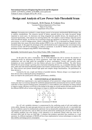
  • 1. International Journal of Engineering Research and Development e-ISSN: 2278-067X, p-ISSN: 2278-800X, www.ijerd.com Volume 8, Issue 2 (August 2013), PP. 19-22 19 Design and Analysis of Low Power Sub-Threshold Sram K.V.Ganesh., B.D.Charan, K.Venkata Siva 1 Assistant Professor,Department of Ece,Vitam 2 Dept of Ece,Vitam. 3 Department of Ece,Vitam . Abstract:- Increasing area overhead is a major design concern in low-power sub-threshold SRAM designs, due to stability considerations. The extensive growth of battery operated devices has made low-power design important in recent years. As electronics are being integrated into portable devices, the demand grows for increased functionality, with reduced size and long battery life. This implies a need to balance ultra-low power with area-efficient design. An obvious way to minimize energy per operation is to decrease VDD. This decreases active power, as well as leakage power, which is affected by DIB. If VDD is decreased too sharply, however, increased delay time causes the power-delay product (PDP) to rise, can be kept minimum if operated in Sub- threshold region. In this paper the advantages of the sub-threshold inverter compared to the conventional strong inversion inverter with 90 nm technology in Cadence is presented. A one-Bit 6T SRAM, sense amplifier, and precharge circuit is designed using HSPICE 45nm technology. Keywords:- Sub-threshold region, Power-Delay Product, DIBL, Temperature, SRAM. I. INTRODUCTION In the past few years a tremendous rise in VLSI fabrication has led to increase the densities of integrated circuits by decreasing the device geometries. Such high density circuits support high design complexities and very high speed but susceptible to power consumption. Circuits with excessive power dissipation are more susceptible to run time failures and give rise to reliability problems. The other factors behind the low power design is growing class of personal computing devices, e.g., as portable desktops, digital pens, audio and video based multimedia products and wireless communications such as PDA’s and smart cards, etc. These devices and systems demand high speed and complex design functionalities. The performance of these devices is Limited by the size, weight and lifetime of portable batteries. Memory design is an integral part in these devices and so reducing the power dissipation in these can improve the system power efficiency, performance, reliability. II. CONVENTIONAL 6T SRAM CELL SRAM have experienced a very rapid development of low power,low voltage memory design during recent years due to an increase demand for notebooks,laptops,hand held communication devices and IC memory cards.Due to these concerns limiting power consumption is a must andhence new techniques are being realised to improve energy efficiency at all levels of the design.In this paper an overall analysis has been carried-out for the different SRAM cells at various technologies in respect to stability and leakage power consumption. Figure 1. Conventional 6T SRAM In a 6T cell, variability tolerance is compromised by the conflicting needs of cell read stability and writes ability. Because the same pass-gate devices are used to both read and write the cell, it is inevitable that the two conditions cannot be simultaneously optimized. Just as dynamically modulated power supplies decouple requirements for read and write, such an effect can also be achieved by modifying the cell itself. The 6T SRAM cell stability problems also arise during a write operation to an unselected column when the word line is activated while both bit lines are held high. A situation that produces equivalent bias conditions to a read operation. So, different topologies of SRAM cell have been implemented at various technologies to improve the data stability and leakage power consumption.
  • 2. DESIGN AND ANALYSIS OF LOW POWER SUB-THRESHOLD SRAM 20 III. 8T SRAM CELL To address the reduced read SNM problem, the read and writeoperations are separated by adding read access structures to the original 6T cell, thus increasing the transistor count to 8. As the read current does not significantly affect the cell value, then the read stability of the 8T cell is dramatically increased compared with the original 6T SRAM cell. The transistor configuration (i.e. M1 through M6) is identical to a conventional 6T SRAM cell. Write access to the cell occurs through the write access transistors and from the write bitlines, BL and BLB. Read access to the cell is through the read access transistor and controlled by the read wordline, RWL. Figure 3.1 shows that the proposed 8T cell has a higher read SNM, comparing to the 6T SRAM cell. Moreover, the write margin of these two cells (defined as the least bitline voltage required to change the state of SRAM cell) is the same due to the unchanged write configuration. However, for the 8T structure, the read bitline leakage is quite significant especially in the deep submicron/Nano ranges. Since it is not possible to design a high-density SRAM using 8T cells, this conclusion leads to an investigation of other cells. Figure 2. 8T SRAM Cell IV. 9TSRAM A 9T structure is proposed in this paper to reduce the powerconsumption of the SRAM cell and the bitline leakage. Figure shows the proposed 9T SRAM cell. Similarly to the 8T cell of, the configuration from M1 to M6 is unchanged (same as in the 6T SRAM cell). The read SNM margin is maintained by retaining the write access circuit and adding a NMOS transistor (M9) between M7 and M8. As shown in, the leakage current through M7, M8, and M9 can be reduced significantly by the so-called stack effect when M7 and M9 are off. Figure 3. 9T SRAM Cell V. 10T SRAM The following figure Shows the schematic of a l0T bitcell that addresses theseproblems and provides sub-threshold functionality. Transistors M1 through M6 are identical to a 6T bitcell except that the source of M3and M6 tie to a virtual supply voltage rail, VVDD. Write access to the bitcell occurs through the write access transistors, M2 and M5, from the write bitlines, BL and BLB. Transistors M7 through M10implement a buffer used for reading. Read access is single-ended and occurs on a separate bitline, RBL, which is precharged prior to read access. The wordline for read also is distinct from the write wordline. One key advantage to separating the read and write wordlines and bitlines is that a memory using this bitcell can have distinct read and write ports. Since a 6T bitcell does not have this feature, the l0T bitcell is in some ways more fairly compared to an 8T dual-port bitcell (6T bitcell with two pairs of access transistors and bitlines). Figure 4. 10T SRAM cell
  • 3. DESIGN AND ANALYSIS OF LOW POWER SUB-THRESHOLD SRAM 21 VI. RESULTS Figure 5. 8T SRAM Write operation Figure 6. 8T SRAM Read operation Figure 7. 9T SRAM Write operation Figure 8 9T SRAM Read operation Figure 6.5: 10T SRAM Write operation Figure 6.6: 10T SRAM Read operation
  • 4. DESIGN AND ANALYSIS OF LOW POWER SUB-THRESHOLD SRAM 22 VII. CONCLUSION In this, I made comparisons between different configurations of SRAMs. In all configurations 4T, 6T, 8T, 9T SRAMs SNM is the problem when scaling the voltages. In 10T SRAM we can find optimum power and optimum delay as well as good SNM. 10 T SRAM achieves best stability and low power compared to remaining configurations in 45nm. Read and write operations done for all configurations. REFERENCES [1] M.E. Sinangil, N. Verma, and A.P. Chandrakasan, ‘‘A Reconfigurable 8T Ultra-Dynamic Voltage Scalable (U-DVS) SRAM in 65 nm CMOS,’’ IEEE J. Solid-State Circuits, vol. 44, no. 11, 2009, pp. 3163-3173. [2] K. Takeda et al., ‘‘A Read-Static-Noise-Margin-Free SRAM Cell for Low-VDD and High-Speed Applications,’’ IEEE J. Solid-State Circuits, vol. 41, no. 1, 2006, pp. 113-121. [3] B.H. Calhoun and A.P. Chandrakasan, ‘‘A 256-kb 65-nm Sub-threshold SRAM Design for Ultra-Low- Voltage Operation,’’ IEEE J. Solid-State Circuits, vol. 42, no. 3, 2007, pp. 680-688 [4] I.J. Chang et al., ‘‘A 32 kb 10T Sub-threshold SRAM Array with Bit-Interleaving and Differential Read Scheme in 90 nm CMOS,’’ IEEE J. Solid-State Circuits, vol. 44, no. 2, 2009, pp. 650-658. [5] H. Pilo et al., ‘‘An SRAM Design in 65-nm Technology Node Featuring Read and Write-Assist Circuits to Expand Operating Voltage,’’ IEEE J. Solid-State Circuits, vol. 42, no. 4, 2007, pp. 813-819. [6] M. Qazi et al., ‘‘A 512kb 8T SRAM Macro Operating down to 0.57V with an AC-Coupled Sense Amplifier and Embedded Data-Retention-Voltage Sensor in 45nm SOI CMOS,’’ Proc. IEEE Int’l Solid-State Circuits Conf. (ISSCC 10), 2010, pp. 350-351. [7] H. Qin et al., ‘‘SRAM Leakage Suppression by Minimizing Standby Supply Voltage,’’ Proc. 5th Int’l Symp. Quality Electronic Design (ISQED 04), IEEE Press, 2004,pp. 55-60. [8] S. Ohbayashi et al., ‘‘A 65-nm SoC Embedded 6T-SRAM Designed for Manufacturability with Read and Write Operation Stabilizing Circuits,’’ IEEE J. Solid-State Circuits, vol. 42, no. 4, 2007, pp. 820- 829. [9] Y. Morita et al., ‘‘An Area-Conscious Low-Voltage- Oriented 8T-SRAM Design under DVS Environment,’’ Proc. IEEE Symp. VLSI Circuits, IEEE Press, 2007, pp. 256-257.