⭐⭐⭐⭐⭐ SOLUCIÓN EVALUACIÓN SISTEMAS DIGITALES 1, 1er Parcial (2021 PAE)
•
0 recomendaciones•9,388 vistas

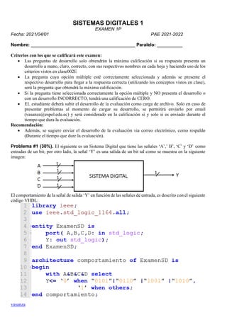
El siguiente es un Sistema Digital que tiene las señales ‘A’,’ B’, ‘C’ y ‘D’ como entradas de un bit; por otro lado, la señal ‘Y’ es una salida de un bit tal como se muestra en la siguiente imagen: El comportamiento de la señal de salida ‘Y’ en función de las señales de entrada, es descrito con el siguiente código VHDL: Realizar los siguientes desarrollos: a) Usando mapas de karnaught y agrupamiento de minterms, simplicar la expresión booleana al mínimo (15p). b) Utilizando puertas lógicas, graficar el circuito que represente a la ecuación simplificada en el literal anterior (15p). ⭐ For more information visit our blog: https://vasanza.blogspot.com/

Más contenido relacionado
La actualidad más candente
La actualidad más candente (20)
Similar a ⭐⭐⭐⭐⭐ SOLUCIÓN EVALUACIÓN SISTEMAS DIGITALES 1, 1er Parcial (2021 PAE)
Similar a ⭐⭐⭐⭐⭐ SOLUCIÓN EVALUACIÓN SISTEMAS DIGITALES 1, 1er Parcial (2021 PAE) (20)
Más de Victor Asanza
Más de Victor Asanza (20)
Último
Último (20)
⭐⭐⭐⭐⭐ SOLUCIÓN EVALUACIÓN SISTEMAS DIGITALES 1, 1er Parcial (2021 PAE)
- 1. vasanza SISTEMAS DIGITALES 1 EXAMEN 1P Fecha: 2021/04/01 PAE 2021-2022 Nombre: _________________________________________ Paralelo: __________ Criterios con los que se calificará este examen: • Las preguntas de desarrollo solo obtendrán la máxima calificación si su respuesta presenta un desarrollo a mano, claro, correcto, con sus respectivos nombres en cada hoja y haciendo uso de los criterios vistos en clase002E • La pregunta cuya opción múltiple esté correctamente seleccionada y además se presente el respectivo desarrollo para llegar a la respuesta correcta (utilizando los conceptos vistos en clase), será la pregunta que obtendrá la máxima calificación. • Si la pregunta tiene seleccionada correctamente la opción múltiple y NO presenta el desarrollo o con un desarrollo INCORRECTO, tendrá una calificación de CERO. • EL estudiante deberá subir el desarrollo de la evaluación como carga de archivo. Solo en caso de presentar problemas al momento de cargar su desarrollo, se permitirá enviarlo por email (vasanza@espol.edu.ec) y será considerado en la calificación si y solo si es enviado durante el tiempo que dura la evaluación. Recomendación: • Además, se sugiere enviar el desarrollo de la evaluación via correo electrónico, como respaldo (Durante el tiempo que dure la evaluación). Problema #1 (30%). El siguiente es un Sistema Digital que tiene las señales ‘A’,’ B’, ‘C’ y ‘D’ como entradas de un bit; por otro lado, la señal ‘Y’ es una salida de un bit tal como se muestra en la siguiente imagen: El comportamiento de la señal de salida ‘Y’ en función de las señales de entrada, es descrito con el siguiente código VHDL:
- 2. vasanza Realizar los siguientes desarrollos: a) Usando mapas de karnaught y agrupamiento de minterms, simplicar la expresión booleana al mínimo (15p). b) Utilizando puertas lógicas, graficar el circuito que represente a la ecuación simplificada en el literal anterior (15p). Resolución: a) b) Problema #2 (30%). El siguiente es un Sistema Digital que tiene las señales ‘A’,’ B’, ‘C’ y ‘D’ como entradas de un bit; por otro lado, la señal ‘Y’ es una salida de un bit tal como se muestra en la siguiente imagen: El comportamiento de la señal de salida ‘Y’ en función de las señales de entrada, es descrito con el siguiente código VHDL:
- 3. vasanza Realizar los siguientes desarrollos: a) Usando mapas de karnaught y agrupamiento de minterms, simplicar la expresión booleana al mínimo (15p). b) Utilizando puertas lógicas, graficar el circuito que represente a la ecuación simplificada en el literal anterior (15p). Resolución: a) b) Problema #3 (30%). El siguiente es un Sistema Digital que tiene las señales ‘A’,’ B’, ‘C’ y ‘D’ como entradas de un bit; por otro lado, la señal ‘Y’ es una salida de un bit tal como se muestra en la siguiente imagen: El comportamiento de la señal de salida ‘Y’ en función de las señales de entrada, es descrito con el siguiente código VHDL:
- 4. vasanza Realizar los siguientes desarrollos: a) Usando mapas de karnaught y agrupamiento de minterms, simplicar la expresión booleana al mínimo (15p). b) Utilizando puertas lógicas, graficar el circuito que represente a la ecuación simplificada en el literal anterior (15p). Resolución: a) b) Problema #4 (30%). El siguiente es un Sistema Digital que tiene las señales ‘A’,’ B’, ‘C’ y ‘D’ como entradas de un bit; por otro lado, la señal ‘Y’ es una salida de un bit tal como se muestra en la siguiente imagen: El comportamiento de la señal de salida ‘Y’ en función de las señales de entrada, es descrito con el siguiente código VHDL:
- 5. vasanza Realizar los siguientes desarrollos: a) Usando mapas de karnaught y agrupamiento de minterms, simplicar la expresión booleana al mínimo (15p). b) Utilizando puertas lógicas, graficar el circuito que represente a la ecuación simplificada en el literal anterior (15p). Resolución: a) b) Problema #5 (x%). El siguiente es un Sistema Digital que tiene las señales ‘A’,’ B’, ‘C’ y ‘D’ como entradas de un bit; por otro lado, la señal ‘Y’ es una salida de un bit tal como se muestra en la siguiente imagen: El comportamiento de la señal de salida ‘Y’ en función de las señales de entrada es la siguiente: Para describir el comportamiento del sistema, se propone utilizar el siguiente código VHDL que está incompleto: Y(A,B,C,D) = ∑ (9,10,12,15) 𝑚
- 6. vasanza Dadas las siguientes opciones, indicar cuál es la correcta asignación de señal para X0, X1, X2 y X3: a) with A&B&C&D select Y<= ‘1’ when “1100”|“1111” |“1001” |“1010”, ‘0’ when others; b) with A&B&C&D select Y<= ‘1’ when “1101”|“1110” |“1000” |“1011”, ‘0’ when others; c) with A&B&C&D select Y<= ‘1’ when “0000”|“0011” |“1100” |“1111”, ‘0’ when others; d) with A&B&C&D select Y<= ‘1’ when “0001”|“0010” |“1101” |“1110”, ‘0’ when others; e) with A&B&C&D select Y<= ‘1’ when “0100”|“0111” |“1000” |“1011”, ‘0’ when others; f) with A&B&C&D select Y<= ‘1’ when “0101”|“0110” |“1001” |“1010”, ‘0’ when others; Resolución: with A&B&C&D select Y<= ‘1’ when “1100”|“1111” |“1001” |“1010”, ‘0’ when others; Problema #6 (x%). El siguiente es un Sistema Digital que tiene las señales ‘A’,’ B’, ‘C’ y ‘D’ como entradas de un bit; por otro lado, la señal ‘Y’ es una salida de un bit tal como se muestra en la siguiente imagen: El comportamiento de la señal de salida ‘Y’ en función de las señales de entrada es la siguiente: Para describir el comportamiento del sistema, se propone utilizar el siguiente código VHDL que está incompleto: Y(A,B,C,D) = ∑ (8,11,13,14) 𝑚
- 7. vasanza Dadas las siguientes opciones, indicar cuál es la correcta asignación de señal para X0, X1, X2 y X3: a) with A&B&C&D select Y<= ‘1’ when “1100”|“1111” |“1001” |“1010”, ‘0’ when others; b) with A&B&C&D select Y<= ‘1’ when “1101”|“1110” |“1000” |“1011”, ‘0’ when others; c) with A&B&C&D select Y<= ‘1’ when “0000”|“0011” |“1100” |“1111”, ‘0’ when others; d) with A&B&C&D select Y<= ‘1’ when “0001”|“0010” |“1101” |“1110”, ‘0’ when others; e) with A&B&C&D select Y<= ‘1’ when “0100”|“0111” |“1000” |“1011”, ‘0’ when others; f) with A&B&C&D select Y<= ‘1’ when “0101”|“0110” |“1001” |“1010”, ‘0’ when others; Resolución: with A&B&C&D select Y<= ‘1’ when “1101”|“1110” |“1000” |“1011”, ‘0’ when others; Problema #7 (x%). El siguiente es un Sistema Digital que tiene las señales ‘A’,’ B’, ‘C’ y ‘D’ como entradas de un bit; por otro lado, la señal ‘Y’ es una salida de un bit tal como se muestra en la siguiente imagen: El comportamiento de la señal de salida ‘Y’ en función de las señales de entrada es la siguiente: Para describir el comportamiento del sistema, se propone utilizar el siguiente código VHDL que está incompleto: Y(A,B,C,D) = ∑ (0,3,12,15) 𝑚
- 8. vasanza Dadas las siguientes opciones, indicar cuál es la correcta asignación de señal para X0, X1, X2 y X3: a) with A&B&C&D select Y<= ‘1’ when “1100”|“1111” |“1001” |“1010”, ‘0’ when others; b) with A&B&C&D select Y<= ‘1’ when “1101”|“1110” |“1000” |“1011”, ‘0’ when others; c) with A&B&C&D select Y<= ‘1’ when “0000”|“0011” |“1100” |“1111”, ‘0’ when others; d) with A&B&C&D select Y<= ‘1’ when “0001”|“0010” |“1101” |“1110”, ‘0’ when others; e) with A&B&C&D select Y<= ‘1’ when “0100”|“0111” |“1000” |“1011”, ‘0’ when others; f) with A&B&C&D select Y<= ‘1’ when “0101”|“0110” |“1001” |“1010”, ‘0’ when others; Resolución: with A&B&C&D select Y<= ‘1’ when “0000”|“0011” |“1100” |“1111”, ‘0’ when others; Problema #8 (x%). El siguiente es un Sistema Digital que tiene las señales ‘A’,’ B’, ‘C’ y ‘D’ como entradas de un bit; por otro lado, la señal ‘Y’ es una salida de un bit tal como se muestra en la siguiente imagen: El comportamiento de la señal de salida ‘Y’ en función de las señales de entrada es la siguiente: Para describir el comportamiento del sistema, se propone utilizar el siguiente código VHDL que está incompleto: Y(A,B,C,D) = ∑ (1,2,13,14) 𝑚
- 9. vasanza Dadas las siguientes opciones, indicar cuál es la correcta asignación de señal para X0, X1, X2 y X3: a) with A&B&C&D select Y<= ‘1’ when “1100”|“1111” |“1001” |“1010”, ‘0’ when others; b) with A&B&C&D select Y<= ‘1’ when “1101”|“1110” |“1000” |“1011”, ‘0’ when others; c) with A&B&C&D select Y<= ‘1’ when “0000”|“0011” |“1100” |“1111”, ‘0’ when others; d) with A&B&C&D select Y<= ‘1’ when “0001”|“0010” |“1101” |“1110”, ‘0’ when others; e) with A&B&C&D select Y<= ‘1’ when “0100”|“0111” |“1000” |“1011”, ‘0’ when others; f) with A&B&C&D select Y<= ‘1’ when “0101”|“0110” |“1001” |“1010”, ‘0’ when others; Resolución: with A&B&C&D select Y<= ‘1’ when “0001”|“0010” |“1101” |“1110”, ‘0’ when others; Problema #9: (x%) Dado la siguiente expresión booleana que define el comportamiento de la señal de salida F sin minimizar, reducir dicha expresión usando mapas de Karnaugh (A, B, C, D) agrupando unos. Luego, seleccionar cuál de las siguientes opciones es la correcta: F = (𝐴 + 𝐵 + 𝐶 + 𝐷)(𝐴 + 𝐵 + 𝐶̅ + 𝐷)(𝐴 + 𝐵 ̅ + 𝐶 + 𝐷)(𝐴 + 𝐵 ̅ + 𝐶̅ + 𝐷) a) 𝑨 + 𝑫 b) 𝑨 ̅ + 𝑫 c) 𝑨 + 𝑫 ̅ d) 𝑨 ̅ + 𝑫 ̅ Resolución:
- 10. vasanza Problema #10: (x%) Dado la siguiente expresión booleana que define el comportamiento de la señal de salida F sin minimizar, reducir dicha expresión usando mapas de Karnaugh (A, B, C, D) agrupando unos. Luego, seleccionar cuál de las siguientes opciones es la correcta: F = (𝐴̅ + 𝐵 ̅ + 𝐶 + 𝐷)(𝐴̅ + 𝐵 ̅ + 𝐶̅ + 𝐷)(𝐴̅ + 𝐵 + 𝐶 + 𝐷)(𝐴̅ + 𝐵 + 𝐶̅ + 𝐷) a) 𝑨 + 𝑫 b) 𝑨 ̅ + 𝑫 c) 𝑨 + 𝑫 ̅ d) 𝑨 ̅ + 𝑫 ̅ Resolución: Problema #11: (x%) Dado la siguiente expresión booleana que define el comportamiento de la señal de salida F sin minimizar, reducir dicha expresión usando mapas de Karnaugh (A, B, C, D) agrupando unos. Luego, seleccionar cuál de las siguientes opciones es la correcta: F = (𝐴̅ + 𝐵 ̅ + 𝐶 + 𝐷 ̅)(𝐴̅ + 𝐵 ̅ + 𝐶̅ + 𝐷 ̅)(𝐴̅ + 𝐵 + 𝐶 + 𝐷 ̅)(𝐴̅ + 𝐵 + 𝐶̅ + 𝐷 ̅) a) 𝑨 + 𝑫 b) 𝑨 ̅ + 𝑫 c) 𝑨 + 𝑫 ̅ d) 𝑨 ̅ + 𝑫 ̅ Resolución:
- 11. vasanza Problema #12: (x%) Dado la siguiente expresión booleana que define el comportamiento de la señal de salida F sin minimizar, reducir dicha expresión usando mapas de Karnaugh (A, B, C, D) agrupando unos. Luego, seleccionar cuál de las siguientes opciones es la correcta: F = (𝐴 + 𝐵 + 𝐶 + 𝐷 ̅)(𝐴 + 𝐵 + 𝐶̅ + 𝐷 ̅)(𝐴 + 𝐵 ̅ + 𝐶 + 𝐷 ̅)(𝐴 + 𝐵 ̅ + 𝐶̅ + 𝐷 ̅) a) 𝑨 + 𝑫 b) 𝑨 ̅ + 𝑫 c) 𝑨 + 𝑫 ̅ d) 𝑨 ̅ + 𝑫 ̅ Resolución: Problema #13: (x%) Dado la siguiente expresión booleana que define el comportamiento de la señal de salida F sin minimizar, reducir dicha expresión usando mapas de Karnaugh (A, B, C, D) agrupando unos. Luego, seleccionar cuál de las siguientes opciones es la correcta: F = (𝐴 + 𝐵 + 𝐶 + 𝐷)(𝐴 + 𝐵 + 𝐶 + 𝐷 ̅)(𝐴̅ + 𝐵 + 𝐶 + 𝐷)(𝐴̅ + 𝐵 + 𝐶 + 𝐷 ̅) a) 𝑪 + 𝑩 b) 𝑪 ̅ + 𝑩 c) 𝑪 + 𝑩 ̅ d) 𝑪 ̅ + 𝑩 ̅ Resolución:
- 12. vasanza Problema #14: (x%) Dado la siguiente expresión booleana que define el comportamiento de la señal de salida F sin minimizar, reducir dicha expresión usando mapas de Karnaugh (A, B, C, D) agrupando unos. Luego, seleccionar cuál de las siguientes opciones es la correcta: F = (𝐴 + 𝐵 + 𝐶̅ + 𝐷 ̅)(𝐴 + 𝐵 + 𝐶̅ + 𝐷)(𝐴̅ + 𝐵 + 𝐶̅ + 𝐷 ̅)(𝐴̅ + 𝐵 + 𝐶̅ + 𝐷) a) 𝑪 + 𝑩 b) 𝑪 ̅ + 𝑩 c) 𝑪 + 𝑩 ̅ d) 𝑪 ̅ + 𝑩 ̅ Resolución: Problema #15: (30%) Se desea diseñar un Sistemas Digital que capaz de controlar dos actuadores tipo bomba (A y B) en función del nivel de agua presente en un tanque. Este nivel de agua se monitorea con dos sensores (S0 y S1). El Sistemas Digital se muestra en la siguiente gráfica:
- 13. vasanza El funcionamiento del sistema digital se detalla a continuación: • El caudal de entrada de agua se abre (A=1) o se cierra (A=0) con el ánimo de controlar el nivel del agua presente en el tanque. Si el nivel del agua es el Mínimo (S1 = 0 y S0 = 1) o menor al mínimo (S1=0 y S0=0) entonces el actuador tipo bomba (A) debe ser abierto (A = 1); por otro lado, si el nivel del agua es el Máximo (S1 = 1 y S0 = 1) entonces el actuador tipo bomba (A) debe ser cerrado (A = 0). • El caudal de salida debe estar abierto (B=1) siempre y cuando el tanque de agua tenga un nivel de agua entre el máximo y el mínimo (S1 =0 y S0 =1) o (S1 =1 y S0 =1). En caso de tener un nivel de agua menor al mínimo (S1 =0 y S0 =0), entonces el caudal de salida debe estar cerrado (B=0). • Recuerde que no es posible que el sensor de nivel máximo (S1) esté detectando agua mientras que el sensor de nivel mínimo (S0) no la detecta (S1=1 y S0=0) Realizar los siguientes desarrollos: a) Completar la siguiente Tabla de Verdad (10p) b) Utilizando mapas de Karnaugh obtener la expresión booleana minimizada de las salidas A y B (10p) c) Utilizando puertas nand de dos entradas hacer el circuito resultante de las salidas A y B (10p) S0 S1 A B 0 0 0 1 1 0 1 1 Resolución: a) S0 (min) S1 (max) A B 0 0 1 0 0 1 Φ Φ 1 0 1 1 1 1 0 1 b)