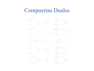
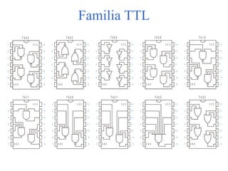
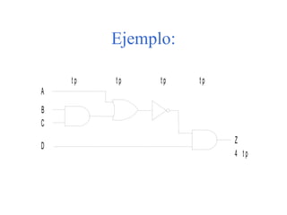
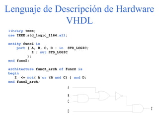
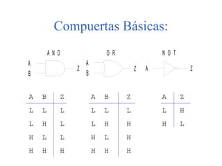
El documento describe circuitos de conmutación formados por compuertas lógicas como AND, OR y NOT. Explica los niveles lógicos de la familia TTL y provee ejemplos de compuertas básicas y compuestas. También cubre el análisis de tiempos de propagación y presenta el lenguaje VHDL para describir circuitos digitales a nivel de hardware.


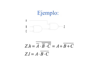
![Ejemplo:
Z
A
B
C
D
[ ]DCBCBA
DCBCBADCBAZ
+⊕⋅⊕⋅
=+⊕+⊕⋅=
)()(
)()(),,,(](https://image.slidesharecdn.com/circuitosdecomunicacin-170630051255/85/Circuitos-de-comunicacion-7-320.jpg)